ENIG FR4 PCB Production Record #FR4-20260515-068
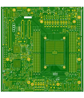
| Parameter | Value | Parameter | Value |
|---|---|---|---|
| PCB Type | FR4 PCB | Quantity | 10 pcs |
| Layers | 14 Layers | Board Type | Panel PCB |
| Dimensions | 244 x 267 mm | Copper Weight | 1oz |
| Thickness | 2 mm | Min Track / Spacing | 4/4mil |
| Surface Finish | ENIG (Immersion Gold) | Min Hole Size | 0.2mm |
| Solder Mask | Green | Silkscreen | White |
| Stack-up | Custom | Impedance Control | Yes |
This 14-layer FR4 PCB fabricated with TG170 material measured 244 × 267 mm at 2.0 mm thickness with 2 oz inner and 1 oz outer copper. Minimum trace and space of 4 mil, combined with impedance control, ENIG finish at 1 µm gold, and resin plugging on selected vias, required multiple engineering file revisions before release. The 10-piece run followed an 18-day factory schedule after panelization in 1×1 format with 5 mm process edges and mechanical routing.
DFM review identified solder-mask openings as small as 3.94 mil, non-metallized hole tolerances too tight for stable control, and uncertainty over which vias required resin plugging versus solder-mask tenting. Additional issues included impedance lines absent from source data, copper features too close to the board edge on layer 3, and non-plated holes drilled through SMD pads. Secondary drilling was applied to preserve pad integrity on those locations, impedance trace widths were adjusted to the verified stack-up, and plugging requirements were clarified on the final production drawings. Copper bridges on the bottom layer were retained only where specified, and edge copper was trimmed to prevent exposure after routing.
All revisions were incorporated into the released files, 100 % flying-probe testing was performed, and the boards shipped complete with electrical test reports and certificates. The process confirmed that the 14-layer TG170 DFM handling maintained required impedance values and via fill integrity across the small lot.
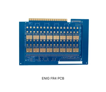
FR4 material with ENIG finish provides balanced electrical performance, shelf life, and assembly compatibility for industrial and high-reliability electronics.
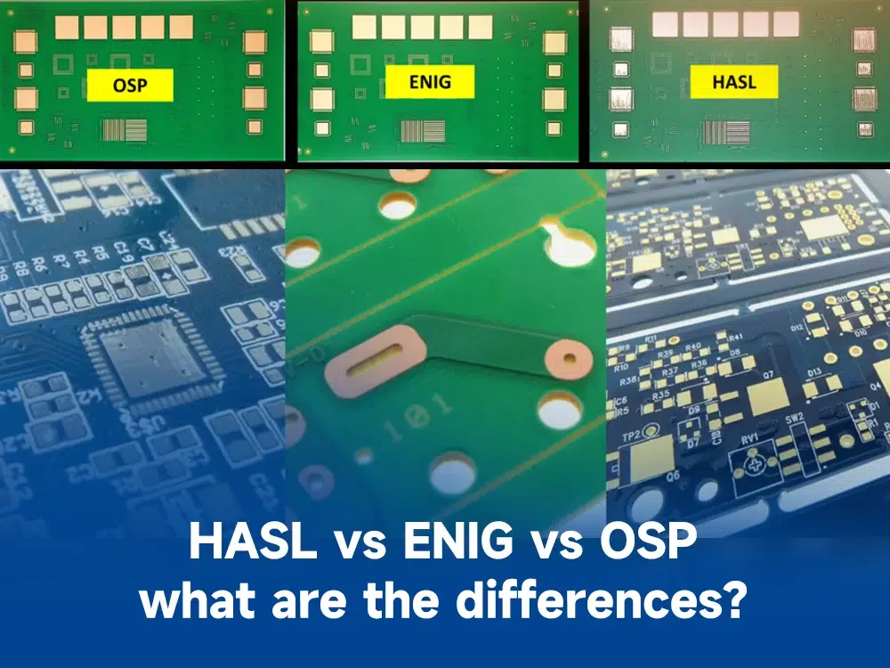
Explore common engineering queries in ENIG, HASL, and OSP FR4 PCBs. Learn real DFM challenges, surface finish compatibility issues, and practical solutions to reduce manufacturing risks and improve yield.
| Order ID | PCB Type | Layers | Dimensions | Solder Mask | Surface Finish | Quantity | Action |
|---|---|---|---|---|---|---|---|
| FR4-20260630-014 | FR4 PCB | 2 | 126 x 145 | Green | ENIG (Immersion Gold) | 10 | View detail |
| FR4-20260529-059 | FR4 PCB | 2 | 147.3 x 53.8 | Green | ENIG (Immersion Gold) | 5 | View detail |
| FR4-20260520-046 | FR4 PCB | 2 | 94.21 x 275 | Green | ENIG (Immersion Gold) | 75 | View detail |


