










A 6-layer FR-4 panel measuring 120 mm × 110.16 mm entered CAM review with a custom stack-up, 1 oz copper, 1.6 mm thickness, green solder mask, white silkscreen, and ENIG finish. Quantity was 20 pieces. Minimum track and space were 5/5 mil and minimum hole size 0.25 mm. The fabrication notes contained a selective resin-plugging instruction limited to the 0.25 mm holes. During data verification the presence of additional vias, openings on larger holes, tight pad spacing, and panel features created overlapping interpretation questions. The central issue that blocked release was the scope of resin filling: the customer note addressed only the smallest holes, while process constraints for a 6-layer ENIG board required a consistent via-plugging strategy across all vias. Until that scope was clarified, the plating, planarization, and solder-mask sequences could not be programmed with confidence.
Design Intent Behind Selective 0.25 mm Via Plugging
The customer's fabrication note instructed resin plugging specifically for the 0.25 mm holes. On a 6-layer board ( #FR4-20260307-058 ) with ENIG and possible via-in-pad structures, selective plugging is sometimes intended to control cost or to leave larger vias open for thermal or electrical reasons. The remaining data, however, showed 0.5 mm holes that carried solder-mask openings, holes whose finished diameter equaled the pad diameter, and internal layer features whose connectivity was ambiguous. The overall design objective appeared to be a compact, high-density 6-layer panel that relied on resin-filled vias for surface planarity under ENIG, yet the written instruction covered only one hole size. This partial definition left the manufacturing path for the rest of the via population undefined.
Selective Resin Plug Note Versus Full Via Population
Our CAM engineer first isolated every via that met or exceeded the 0.25 mm threshold. The note addressed only the smallest diameter. In actual 6-layer processing with ENIG, resin plugging is typically applied to the entire via population when surface planarity or via-in-pad reliability is required. Leaving larger vias unplugged while via plugging only the 0.25 mm holes would create mixed surface topography: some vias filled and planarized, others open and recessed. Under subsequent solder-mask and ENIG steps the height difference can produce uneven plating thickness, incomplete mask coverage, or solder voids at assembly. The factory therefore proposed extending resin plugging to all vias so that a single, consistent process window could be used.
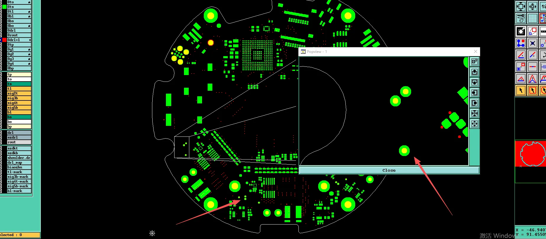
Figure 1: plug the via with resin
If the selective instruction had been followed literally, two realistic outcomes were possible. First, the unplugged vias would remain open after plating, allowing solder or flux entrapment during assembly and increasing the risk of outgassing or reliability failures. Second, the mixed filled/unfilled surface would complicate solder-mask application and ENIG thickness control, potentially violating IPC-6012 surface-finish uniformity expectations. Either result would have compromised yield on a 20-piece panel run.
| Via Population | Customer Note | Factory Process Need | Risk if Selective Only |
|---|---|---|---|
| 0.25 mm holes | Resin plug required | Resin plug | None if followed |
| Larger vias (incl. 0.5 mm) | Not addressed | Resin plug for consistency | Mixed topography, plating variation |
| Holes equal to pad size | Unclear | Treat as NPTH or confirm plating | Incorrect plating attribute |
Primary Conflict: Incomplete Resin Filled Via Definition
The dominant conflict was a design-intent ambiguity combined with a manufacturing-interpretation conflict. The fabrication note supplied a partial resin-plugging rule limited to 0.25 mm holes, while the actual via population and the process requirements of a 6-layer ENIG board demanded a uniform strategy. IPC-4761 describes several via-filling types; when the customer specifies only one diameter, the factory cannot assume the remaining vias should remain open or receive a different treatment. On this panel the presence of solder-mask openings over 0.5 mm holes further blurred whether those features were intended as open vias or as plugged structures whose openings should be closed after filling.
Because the FR4 board used a custom stack-up and ENIG, surface planarity after via filling directly affected final plating uniformity and solder-mask registration. Leaving the scope unresolved would have forced the process engineers to choose between two incompatible flows: selective plugging that matched the note but created topography issues, or full plugging that matched process capability but exceeded the written instruction. Production therefore could not proceed until the customer confirmed the intended via-filling population.
Supporting Issues That Reinforced Via Clarification Need
Several secondary observations supported the primary concern. Holes of 0.5 mm carried solder-mask openings; without confirmation it was unclear whether they were open vias or features that should be tented or plugged. On layer 3 certain copper features appeared partially connected, raising the possibility of an incomplete net or a drafting artifact. Pad-to-pad spacing in one region fell below the minimum required for a reliable solder-mask bridge, risking mask web breakage. The panel contained routing slots whose relationship to stamp-hole (mouse-bite) features was undefined. Finally, certain holes matched pad diameter exactly and were therefore candidates for NPTH treatment, and the overall board dimensions stated in the specification file did not match the Gerber outline. Each of these points required its own confirmation, yet all of them interacted with the via-filling decision: once the resin-plug scope was locked, the remaining attributes could be resolved against a consistent process baseline.
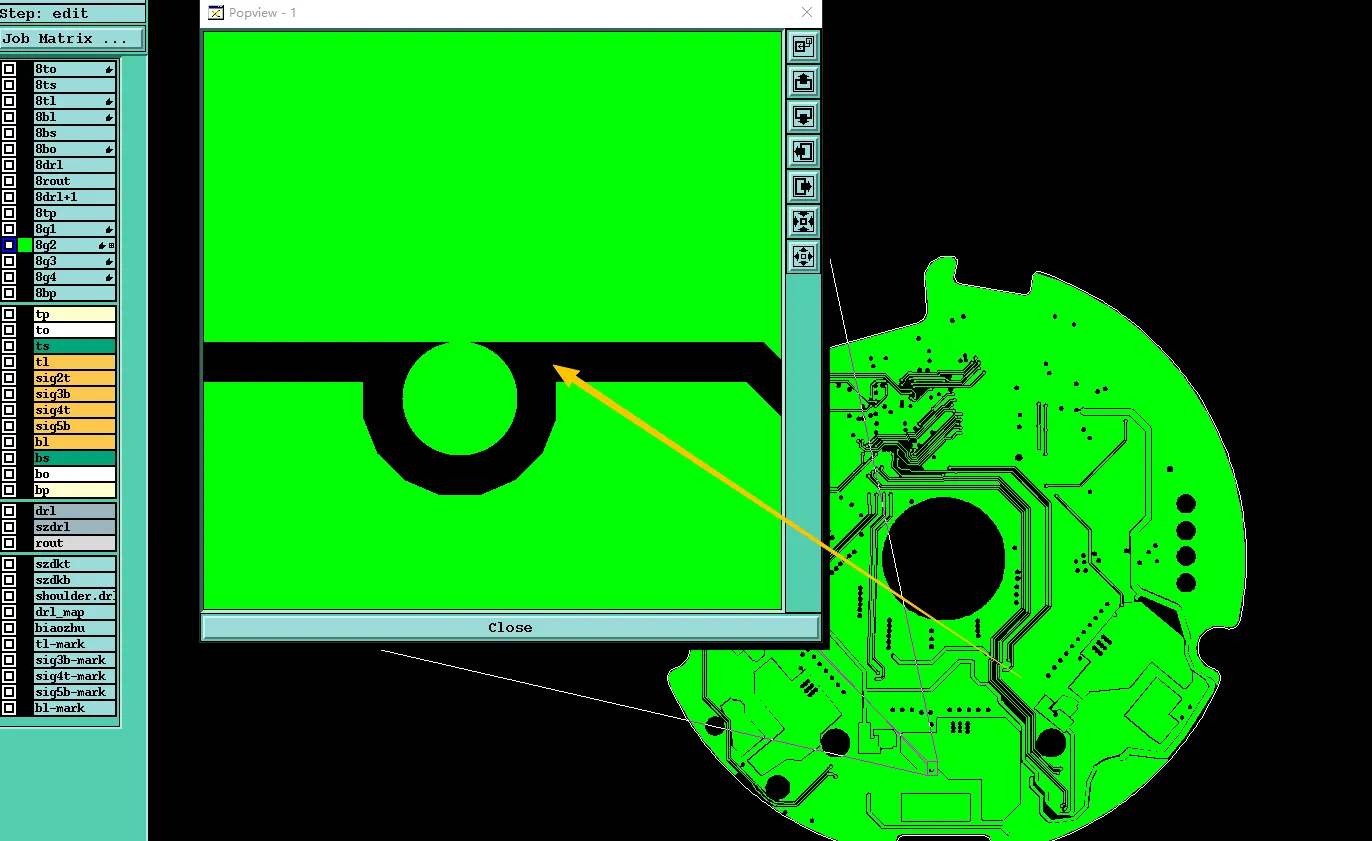
Figure 2: the dot be connected to the adjacent copper
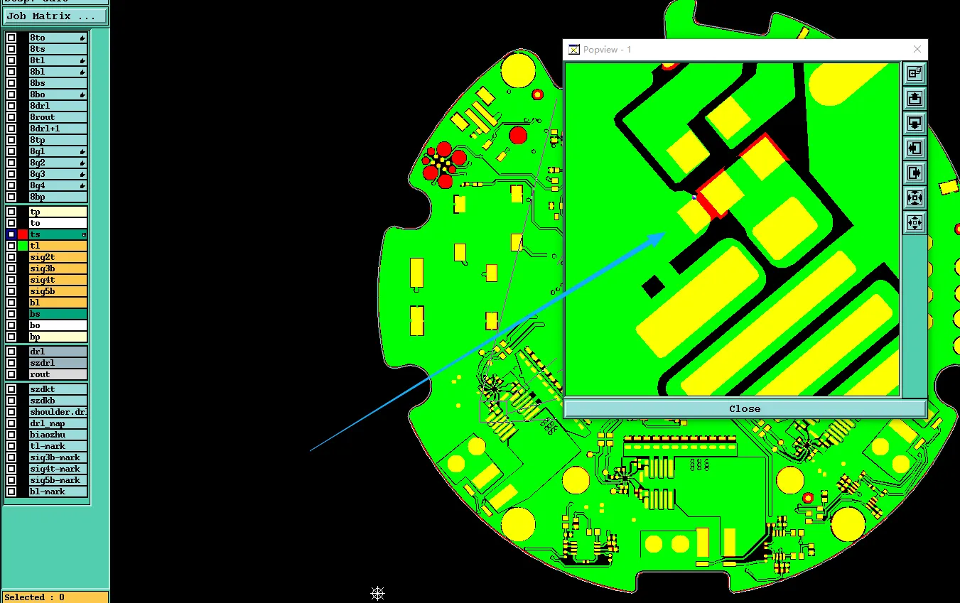
Figure 3: the two pads are too close together to make a solder mask river
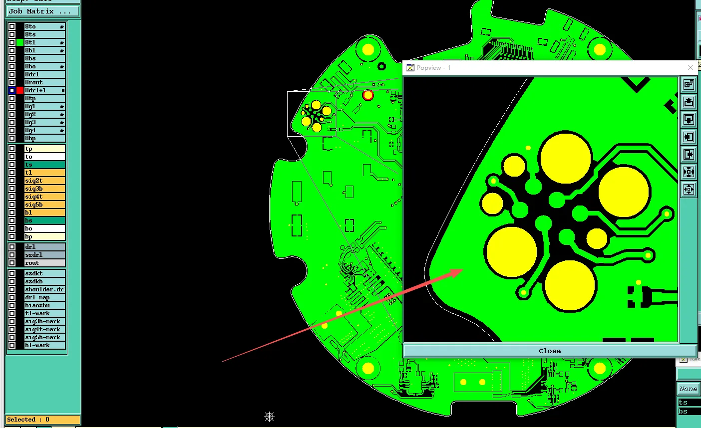
Figure 4: certain holes matched pad diameter exactly
Customer Confirmation of Full Via Resin Plugging
The engineering reply presented a single, coherent proposal. All vias, regardless of diameter, would receive non-conductive resin plugging followed by planarization so that the subsequent ENIG and solder-mask steps would encounter a uniform surface. The 0.5 mm holes with openings would be treated as vias and included in the plugging process; after filling the openings would be evaluated for tenting or residual exposure according to the final mask data. Holes whose diameter equaled the pad would be re-attributed as NPTH unless the customer directed otherwise. The tight pad spacing would be accepted with the understanding that a solder-mask bridge might not form, and the panel routing slots would be processed as designed while stamp-hole intent was clarified. Dimension discrepancies would be resolved by adopting the Gerber outline as the manufacturing authority.
Customer confirmation accepted the full via resin-plugging scope and the accompanying attribute decisions. The CAM data were updated to apply resin fill to the entire via population, NPTH attributes were assigned where hole and pad diameters matched, and the outline was locked to the Gerber dimensions. With a single via-filling strategy in place, the remaining secondary issues were closed without further process conflict. The 6-layer panel was released for production.
| Engineering Observation | Conflict Identified | Recommended Action | Final Status |
|---|---|---|---|
| Note limited resin plug to 0.25 mm holes | Incomplete via-filling scope | Extend resin plug to all vias | Confirmed |
| 0.5 mm holes with mask openings | Via versus non-via ambiguity | Treat as vias and include in plugging | Confirmed |
| Holes equal to pad diameter | Plating attribute unclear | Process as NPTH | Confirmed |
| Pad spacing below mask-bridge minimum | Solder-mask dam risk | Accept possible missing bridge | Noted |
Design Lessons for Consistent Resin Filled Via Specification
- When resin plugging is required, state the rule for the entire via population rather than a single diameter; selective instructions force process interpretation.
- On 6-layer ENIG boards, mixed filled and unfilled vias create surface topography that complicates plating uniformity and solder-mask application.
- Holes that carry solder-mask openings should be explicitly identified as open vias or as features intended for plugging and subsequent tenting.
- Holes whose finished diameter equals the pad diameter are normally treated as NPTH unless a plating requirement is stated.
- Pad-to-pad spacing must allow a reliable solder-mask bridge if mask dams are required; otherwise the design must accept possible copper exposure.
- Panel routing slots and stamp-hole features should be defined together so that depanelization method is unambiguous.
- Specification-file dimensions must match the Gerber outline; any discrepancy will halt CAM until the controlling source is confirmed.
- Reference IPC-4761 via-filling types in the fabrication notes when a specific plugging method is intended, reducing the need for later clarification.
FAQ
Q1: Why does a note that plugs only 0.25 mm holes trigger an Engineering Question on a 6-layer board?
A1: Process consistency for ENIG and solder mask normally requires the same treatment for all vias. Selective plugging creates mixed surface heights that risk plating and mask defects.
Q2: What is the risk of leaving larger vias unplugged while plugging only the smallest holes?
A2: The resulting topography can cause uneven ENIG thickness, incomplete solder-mask coverage, and potential solder voids or outgassing at assembly.
Q3: How should 0.5 mm holes with solder-mask openings be treated when resin plugging is in use?
A3: They should be confirmed as vias and included in the plugging process; after filling the openings can be tented or left according to the final mask data.
Q4: Why are holes equal in size to their pads normally processed as NPTH?
A4: Equal hole and pad diameters leave no annular ring for reliable plating adhesion. Unless plating is explicitly required, NPTH avoids weak or incomplete copper barrels.
Q5: Can a factory form a solder-mask bridge when pad spacing is below the process minimum?
A5: No. The mask web will not form reliably. The design must either increase spacing or accept the possibility of exposed copper between pads.
Q6: Why must specification-file dimensions match the Gerber outline?
A6: CAM uses the Gerber data to generate the routing path. Any mismatch requires confirmation of which source defines the finished board size before tooling is released.
```






