










PCB Specifications
| Parameter | Value | Parameter | Value |
|---|---|---|---|
| PCB Type | FR4 PCB | Quantity | 20 pcs |
| Layers | 6 Layers | Board Type | Panel PCB |
| Dimensions | 120 x 110.16 mm | Copper Weight | 1oz |
| Thickness | 1.6 mm | Min Track / Spacing | 5/5mil |
| Surface Finish | ENIG (Immersion Gold) | Min Hole Size | 0.25mm |
| Solder Mask | Green | Silkscreen | White |
| Stack-up | Custom | Impedance Control | No |
Manufacturing Timeline
Logistics Information
Key Manufacturing Processes
Manufacturing Summary
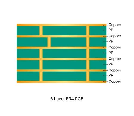
This 6-layer FR-4 board measured 120 × 110.16 mm with 1.6 mm thickness, TG170 material, and 1 oz copper on both sides. Produced as 20 pieces in 2×2 panels for 5 sets, the order used ENIG surface finish, green solder mask, and white silkscreen. The design featured tight 5 mil line/space geometry and 0.25 mm minimum holes. Customer notes required epoxy filling and capping of all 0.25 mm vias, with 4 mm process edges supporting routing separation. The 10-day schedule included 100% flying probe testing.
DFM review addressed several via and panel details. Although the order specified resin plugging only for 0.25 mm holes, process capability required vias plugging for consistent reliability; this was confirmed. Certain 0.5 mm holes carried openings in the original data and needed clarification of via status. Layer-3 features appeared partially connected and required explicit processing instructions. Tight pad spacings prevented formation of solder-mask bridges. Panel routing slots were reviewed to confirm whether stamp-hole bridge construction applied. Holes equal in size to their pads were designated NPTH, and dimensional inconsistencies between the drawing and Gerber data were resolved.
Confirmed via plugging scope, NPTH designation, and panel configuration were implemented prior to production. The boards achieved consistent ENIG plating and reliable resin plugging reliability handling across the 6-layer stack. Full electrical test reports and quality certificates accompanied the shipment, confirming the panels met the specified mechanical and electrical requirements.
Explore More PCB Manufacturing Resources
6 Layer FR4 PCB Manufacturing Insights
Discover how AIVON manufactures 6 Layer FR4 PCBs, including multilayer stackup optimization, impedance control requirements, fabrication processes, manufacturing challenges, and real production experience from customer orders.

How to Avoid Common Engineering Queries in Multilayer FR4 PCB Design
Real multilayer FR4 PCB CAM review cases covering stack-up confirmation, impedance control, copper balance, via tenting, and edge clearance EQs. Discover practical DFM best practices for 4-layer and higher boards to reduce engineering queries, prevent warpage, and improve first-pass yield.
Real Production Records
| Order ID | PCB Type | Layers | Dimensions | Solder Mask | Surface Finish | Quantity | Action |
|---|---|---|---|---|---|---|---|
| FR4-20260819-043 | FR4 PCB | 10 | 157 x 140 | Blue | ENIG (Immersion Gold) | 100 | View detail |
| FR4-20260818-014 | FR4 PCB | 2 | 110.32 x 173.3 | Green | ENIG (Immersion Gold) | 200 | View detail |
| FR4-20260811-033 | FR4 PCB | 8 | 226.8 x 10⁹ | Green | ENIG (Immersion Gold) | 50 | View detail |


