










PCB Specifications
| Parameter | Value | Parameter | Value |
|---|---|---|---|
| PCB Type | FR4 PCB | Quantity | 200 pcs |
| Layers | 2 Layers | Board Type | Panel PCB |
| Dimensions | 110.32 x 173.3 mm | Copper Weight | 1oz |
| Thickness | 1.6 mm | Min Track / Spacing | 5/5mil |
| Surface Finish | ENIG (Immersion Gold) | Min Hole Size | 0.25mm |
| Solder Mask | Green | Silkscreen | White |
| Stack-up | Custom | Impedance Control | No |
Manufacturing Timeline
Logistics Information
Key Manufacturing Processes
Manufacturing Summary
Production of 200 panels of 2-layer FR4 circuit boards sized 110.32 x 173.3 mm proceeded with 1.6 mm board thickness, 1 oz copper weight, and a custom stackup. The tighter 5/5 mil track and spacing required precise control in the circuit imaging and etching stages to achieve accurate feature definition. Minimum hole size of 0.25 mm was maintained throughout drilling and plating operations for this panelized configuration.
Green soldermask combined with white silkscreen preceded the surface finish. Electroless nickel deposition and immersion gold deposition created a uniform ENIG layer, delivering reliable pad surfaces for PCB assembly. Comprehensive electrical testing validated each panel prior to shipment.
The manufacturing sequence was executed over 2.2 days, resulting in consistent quality and adherence to all design parameters for these boards.
This order also received positive feedback from the customer regarding the consistent quality and reliable delivery. View the full customer review→
Explore More PCB Manufacturing Resources
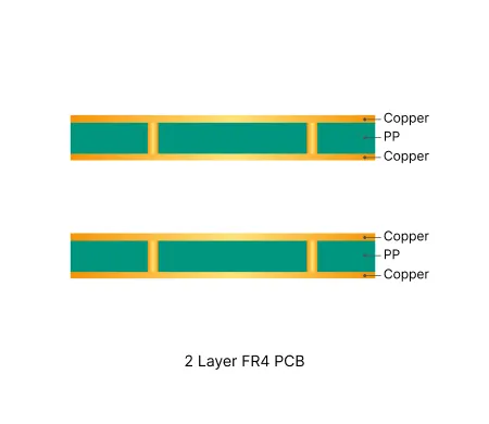
2 Layer FR4 PCB Manufacturing Insights
Discover how AIVON manufactures 2 Layer FR4 PCBs, including double-sided circuit structures, reliable through-hole fabrication processes, manufacturing challenges, and real production experience from customer orders.
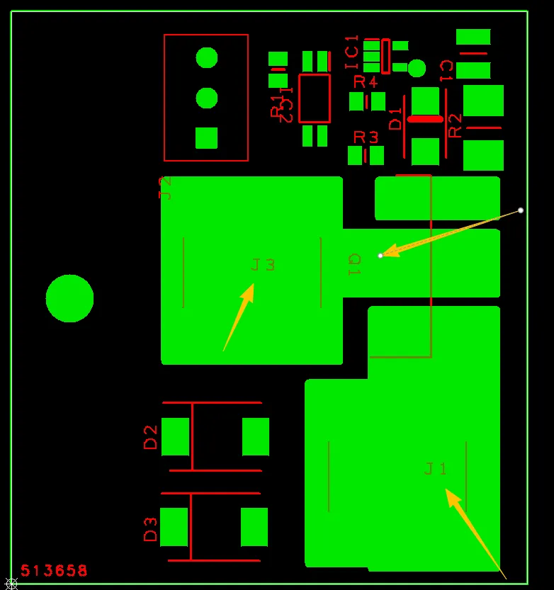
Common Engineering Queries in 2 Layer FR4 PCB Design and Manufacturing
Real Engineering Queries (EQ) and DFM issues for 2 Layer FR4 PCB (double-sided boards) from actual production reviews. Learn how to avoid common problems with via treatment, silkscreen on pads, solder mask openings, hole attributes, board edge clearance, and other frequent design pitfalls.
Real Production Records
| Order ID | PCB Type | Layers | Dimensions | Solder Mask | Surface Finish | Quantity | Action |
|---|---|---|---|---|---|---|---|
| FR4-20261007-048 | FR4 PCB | 2 | 99.04 x 75.87 | Matte Black | HASL Lead Free | 15 | View detail |
| FR4-20261007-047 | FR4 PCB | 2 | 92.84 x 72.52 | Green | HASL Lead Free | 5 | View detail |
| FR4-20261007-046 | FR4 PCB | 2 | 65 x 97 | Green | HASL Lead Free | 5 | View detail |


