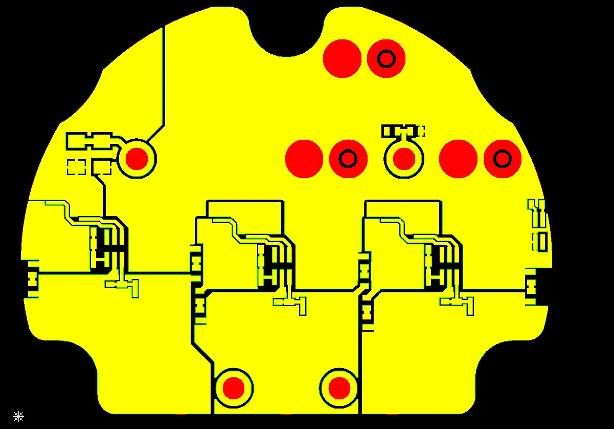
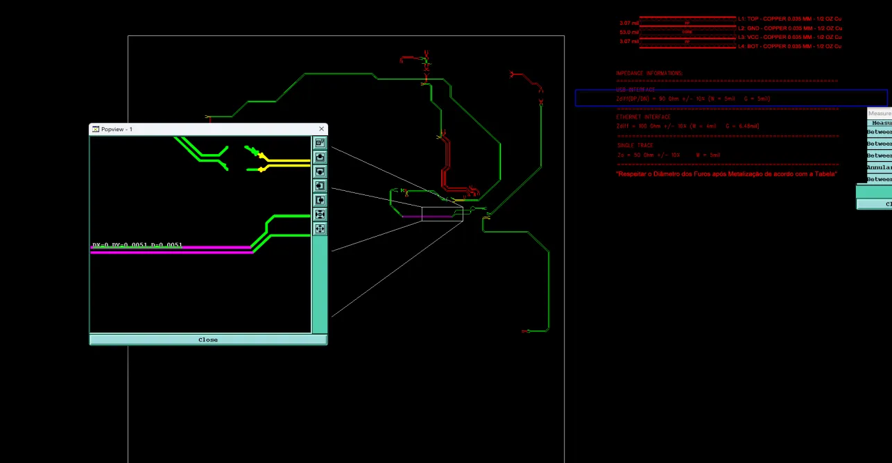
During CAM review of a 4-layer FR-4 board measuring 129.5 mm by 160 mm with a high hole density of 54 500 per square meter, our engineering team identified multiple vias located directly inside component pads. From a DFM perspective, this Via-in-Pad configuration without any fill process created an immediate risk of solder wicking, pad voids, and cold joints during SMT assembly. The primary concern was manufacturing stability and long-term solder-joint reliability rather than basic fabricability. Without clarification, the finished boards could have entered assembly with defective pads that produce intermittent opens or complete joint failure under thermal stress. This case provides practical insight into PCB Via-in-Pad Design Rules for high-density 4-layer constructions.
The order ( #FR4-20260202-040 ) specified FR-4 (KB-6160), TG130, 1.6 mm thickness, 1 oz copper on all layers, black solder mask on both sides, white silkscreen, immersion gold finish at 1 µin with 13.4 % gold area, customer self-panelization using V-cut, no process edge, impedance control required, 100 % flying-probe testing, and a four-day delivery window. Quantity was 600 pieces. These parameters are common for compact, high-density designs, yet the combination of Via-in-Pad features, pads approaching the board outline, NPTH holes with copper pads, and tight IC spacing required explicit engineering confirmation before production release.
Why Via-in-Pad and Edge Features Triggered Immediate DFM Scrutiny
Our CAM engineer began by overlaying the drill data against the outer copper and solder-mask layers. Multiple vias were found centered or partially inside SMT pads. On a board with 0.25 mm holes and 5 mil line/space rules the plated via barrels occupy a significant portion of the pad area. After plating and immersion gold the pad surface becomes discontinuous, leaving cavities that trap air or allow solder paste to wick away during reflow.
Additional observations included circuit pads lying closer to the outline than the safe clearance for V-cut (normally ≥0.4 mm) and contour routing (normally ≥0.2 mm), NPTH holes that still carried copper pads on both sides, copper holes without solder-mask openings, IC pad spacing below 8 mil that threatened solder mask bridge formation, and a square slot that could not be produced with available tooling. Positioning holes were also clustered on one side, raising handling concerns.
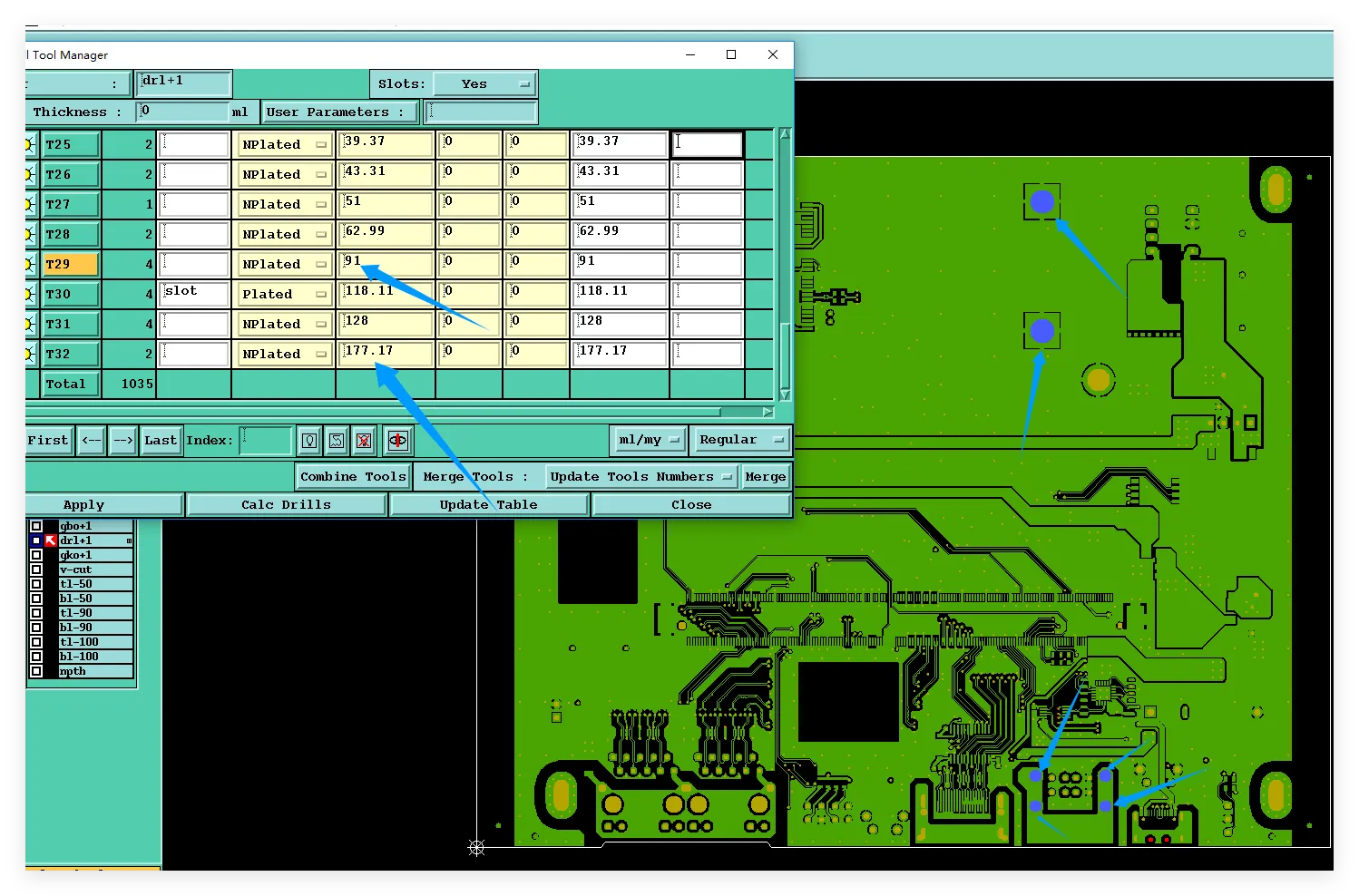
Figure 1: NPTH holes that still carried copper pads on both sides
Risk indicators included the high hole density, customer V-cut panelization with zero process edge, short four-day lead time, and the presence of active Via-in-Pad features without any fill or planarization call-out. These factors combined to create both assembly and edge-integrity risks that could not be left unresolved.
| Feature Observed | Condition in Files | Primary DFM Risk |
|---|---|---|
| Vias inside component pads | Multiple locations, no fill | Solder wicking and cold joints |
| Pads to board outline | Below 0.2 / 0.4 mm clearance | Exposed copper after V-cut |
| NPTH with copper pads | Attribute conflict | Unexpected plating or pad damage |
Table 1 records the key observations that generated the Engineering Question.
Via-in-Pad, Edge Clearance and Mask Bridge Risks Identified
The highest-priority risk was the presence of vias inside SMT pads without resin fill or plated-over via fill. After plating the via barrel creates a cavity within the pad. During reflow solder paste can disappear into the open hole, producing voids, incomplete fillets, or cold joints that later fail under thermal cycling. The second major risk involved pads and copper features lying too close to the board outline on a V-cut panel with no process edge; after scoring and contour the remaining copper would be left exposed or lifted. The third risk concerned IC pad spacing below 8 mil, which left insufficient room for a reliable solder-mask dam and increased the chance of solder bridging.
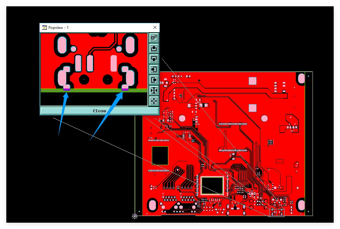
Figure 2: the pad is too close to the outline
Secondary issues included NPTH holes that still carried copper pads on both sides (creating an attribute conflict), copper holes without solder-mask openings, a square slot that could not be drilled, and one-sided positioning holes that complicated panel handling. These required confirmation but did not carry the same immediate assembly-critical weight as the Via-in-Pad and edge-clearance problems.
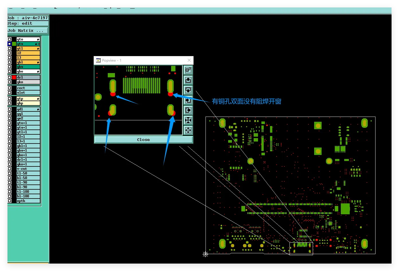
Figure 3: copper holes without solder-mask openings
From a DFM perspective the priority sequence was clear: decide how to treat the Via-in-Pad features, restore safe edge clearances, and confirm solder-mask bridge feasibility before any tooling was released.
How Open Via-in-Pad Features Compromise Solder Joint Integrity
If production had continued without addressing the open vias inside pads, the finished immersion-gold surfaces would have contained cavities or residual plating depressions. During SMT the solder paste would partially wick into the via barrels, leaving insufficient solder volume for a reliable joint. The result is cold solder joints, voids, or intermittent opens that may pass initial electrical test yet fail after thermal cycling or mechanical stress. On a 4-layer board with impedance control these defects can also introduce local signal discontinuities.
According to common IPC-A-600 acceptability considerations and practical PCB assembly experience, open vias under active pads are a known source of solder-joint defects. When the via is left unfilled the capillary action of molten solder pulls material away from the joint, reducing fillet strength and increasing the probability of field failures.
Pads left too close to the V-cut or contour edge produce exposed copper, burrs, or lifted copper after mechanical forming. These edge defects fail visual inspection and can create shorting paths against metal enclosures. IC pad spacing below 8 mil further raises the risk of solder-mask bridge failure, allowing solder to bridge adjacent pads during reflow.
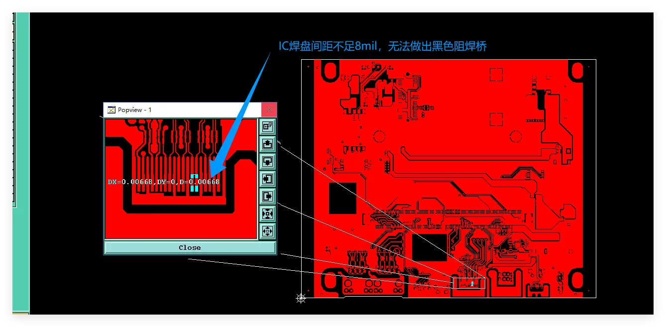
Figure 4: IC pad spacing below 8 mil
| Potential Failure Mode | Root Cause Linked to EQ | Production or Field Impact |
|---|---|---|
| Solder wicking and cold joints | Open vias inside SMT pads | Assembly rejects, intermittent opens |
| Exposed copper at edge | Pads closer than 0.2 / 0.4 mm | Visual scrap, shorting risk |
| Solder bridging | IC spacing below 8 mil | Short circuits after reflow |
| Pad surface voids | Unfilled Via-in-Pad | Weak joints under thermal stress |
Table 2 maps each realistic failure mode to the Engineering Question items.
Failure Scenarios the Engineering Team Sought to Prevent
Had the vias remained open inside the SMT pads, boards reaching the assembly line would have shown incomplete pad surfaces. Solder paste would wick into the barrels, producing voids that weaken the joint. Under subsequent thermal cycling the joints could crack or lift, generating field failures that are difficult to attribute to the original via design. On an impedance-controlled 4-layer board these intermittent opens also degrade signal integrity.

Figure 5: via-in-pad design
Leaving pads too close to the outline would have produced exposed copper, burrs, or lifted copper after V-cut and contour. These edge defects fail visual criteria under IPC-A-600 and create potential shorting paths. IC pad spacing below 8 mil would have allowed solder-mask dams to break or disappear, resulting in solder bridges during reflow.
NPTH holes carrying copper pads would have created an attribute conflict: either unexpected plating or damaged pads after non-plated processing. A square slot without rounded corners could not be produced, forcing a late design change under the four-day schedule. All of these scenarios share a common origin: insufficient design-for-manufacturing detail at the via, edge, and mask interfaces.
Preventive Actions Confirmed During the DFM Exchange
Our engineering team issued a prioritized Engineering Question that first addressed the Via-in-Pad features. The recommendation was to apply resin-filled vias (or plated-over via fill) followed by planarization so that the pad surfaces would remain continuous and free of cavities. This process restores a flat, solderable surface and eliminates the risk of solder wicking.
For pads too close to the outline the team requested either copper pull-back to meet the 0.2 mm (routing) / 0.4 mm (V-cut) minimums or explicit acceptance of limited edge exposure. NPTH holes carrying copper pads were flagged for attribute clarification so that plating and mask treatment would match design intent. Copper holes without solder-mask openings were confirmed for treatment (tented, opened, or filled). IC spacing below 8 mil was reviewed for possible mask-bridge feasibility or minor pad adjustment. The square slot was proposed with R0.4 mm rounded corners to match available tooling. Positioning-hole placement was noted for handling improvement.
With customer confirmation on the critical Via-in-Pad treatment, edge clearances, and remaining items, the CAM data were updated and the order released under the four-day schedule. The revised design retained all electrical and impedance performance while eliminating the primary sources of assembly defects and edge damage.
| Action Item | Customer Decision Direction | Manufacturing Benefit |
|---|---|---|
| Via-in-Pad features | Resin fill / planarization recommended | Continuous pad surface, no solder voids |
| Pads to outline clearance | Pull-back or limited exposure accepted | No exposed copper after V-cut |
| IC pad spacing | Bridge feasibility confirmed | Reduced solder-bridging risk |
Table 3 documents the closed decisions that converted a high-risk Via-in-Pad design into a manufacturable and assembly-ready product.
Building Trust Through Early Via and Edge Verification
This case demonstrates that open Via-in-Pad features on high-density 4-layer boards are not minor layout details; they constitute a direct threat to solder-joint integrity and long-term reliability. By identifying the unfilled vias inside SMT pads during CAM review and confirming a fill-and-planarize approach, the engineering team protected both first-pass assembly yield and field performance. Explicit treatment of edge clearances, NPTH attributes, and mask-bridge limits further reduced the chance of late-stage rejects under a tight four-day schedule.
Designers working with high-hole-density FR-4 boards are encouraged to avoid open vias under active pads or to specify resin fill / plated-over via fill, maintain adequate copper-to-outline clearances for V-cut panels, keep IC pad spacing compatible with solder-mask dams, and request early DFM feedback on via treatment and edge features. These practices convert potential manufacturing and assembly problems into controlled, documented decisions before production begins.
Proactive verification of Via-in-Pad design rules remains one of the highest-leverage actions a DFM team can take when releasing high-density multilayer boards.
FAQ
Q1: Why do open vias inside SMT pads create cold-joint risks?
A1: The plated via barrel forms a cavity within the pad. During reflow, molten solder is drawn into the hole by capillary action, leaving insufficient solder volume for a strong fillet. The resulting joint can appear acceptable initially yet fail under thermal cycling.
Q2: What is the recommended treatment for Via-in-Pad features on high-density boards?
A2: Resin-filled vias followed by planarization, or plated-over via fill (POVF), restore a continuous, flat pad surface. This prevents solder wicking and provides a reliable soldering platform for fine-pitch components.
Q3: Why must pads maintain minimum clearance to V-cut and contour edges?
A3: V-cut and routing tools remove material at the defined outline. Pads closer than approximately 0.4 mm (V-cut) or 0.2 mm (routing) are left with exposed copper, burrs, or lifted copper that fail visual inspection and create shorting hazards.
Q4: How does IC pad spacing below 8 mil affect solder-mask bridges?
A4: Narrow gaps leave insufficient room for a stable solder-mask dam. The dam can break or disappear during processing, allowing solder to bridge adjacent pads during reflow and create short circuits.
Q5: Can open Via-in-Pad features pass electrical test yet still fail in the field?
A5: Yes. Initial continuity may exist, but the weakened solder joint can crack or lift after thermal cycling or mechanical stress, producing intermittent opens that appear only after the product is in service.
Q6: How can designers avoid similar issues on future high-density boards?
A6: Keep vias outside active SMT pads or specify resin fill / plated-over via fill, maintain adequate copper-to-outline clearances for V-cut panels, ensure IC pad spacing supports reliable solder-mask dams, and request early DFM review of via treatment and edge features. These steps form the practical foundation of PCB Via-in-Pad Design Rules.