










PCB Specifications
| Parameter | Value | Parameter | Value |
|---|---|---|---|
| PCB Type | FR4 PCB | Quantity | 600 pcs |
| Layers | 4 Layers | Board Type | Panel PCB |
| Dimensions | 129.5 x 160 mm | Copper Weight | 1oz |
| Thickness | 1.6 mm | Min Track / Spacing | 5/5mil |
| Surface Finish | ENIG (Immersion Gold) | Min Hole Size | 0.25mm |
| Solder Mask | Black | Silkscreen | White |
| Stack-up | Custom | Impedance Control | Yes |
Manufacturing Timeline
Logistics Information
Key Manufacturing Processes
Manufacturing Summary
This 4-layer FR-4 board measured 129.5 × 160 mm with 1.6 mm thickness, TG130 material, and 1 oz copper on both sides. Produced as 600 pieces in customer 1×1 panels, the order used ENIG surface finish, black solder mask, and white silkscreen. The design included controlled impedance with a minimum line/space of 5 mil and 0.25 mm holes. V-cut separation was applied without process edges, and the 4-day schedule required 100% flying probe testing on the high-density layout.
DFM review resolved multiple hole, mask, and edge constraints. Non-plated holes concentrated on one side complicated board fixturing; using plated holes for location risked wall damage and discoloration. Several holes defined as NPTH still carried pads on both sides, requiring attribute clarification. Certain plated holes lacked solder-mask openings on either side. Pads and copper approached the outline closer than the minimum clearances for routing (0.2 mm) and V-cut (0.4 mm), creating risk of exposed copper, burrs, or lifted foil after forming. Square slots could not be produced with available tooling and were proposed with R0.4 mm rounded corners. IC pad spacings below 8 mil prevented reliable solder-mask bridges, and via-in-pad features raised potential solder-joint concerns during PCB assembly.
Confirmed hole attributes, edge clearances, slot geometry, and mask-window decisions were implemented prior to production. The boards achieved consistent ENIG plating and controlled-impedance performance across the full quantity within the accelerated timeline. Full electrical test reports and quality certificates accompanied the shipment, confirming the panels met the specified mechanical and electrical requirements.
Explore More PCB Manufacturing Resources
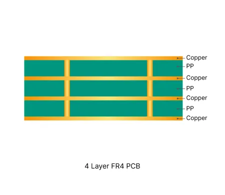
4 Layer FR4 PCB Manufacturing Insights
Discover how AIVON manufactures 4 Layer FR4 PCBs, including multilayer stackup design, layer alignment control, fabrication processes, manufacturing challenges, and real production experience from customer orders.

How to Avoid Common Engineering Queries in Multilayer FR4 PCB Design
Real multilayer FR4 PCB CAM review cases covering stack-up confirmation, impedance control, copper balance, via tenting, and edge clearance EQs. Discover practical DFM best practices for 4-layer and higher boards to reduce engineering queries, prevent warpage, and improve first-pass yield.
Real Production Records
| Order ID | PCB Type | Layers | Dimensions | Solder Mask | Surface Finish | Quantity | Action |
|---|---|---|---|---|---|---|---|
| FR4-20260911-001 | FR4 PCB | 4 | 76.33 x 49.91 | Green | HASL Lead Free | 10 | View detail |
| FR4-20260819-043 | FR4 PCB | 10 | 157 x 140 | Blue | ENIG (Immersion Gold) | 100 | View detail |
| FR4-20260818-014 | FR4 PCB | 2 | 110.32 x 173.3 | Green | ENIG (Immersion Gold) | 200 | View detail |


