Introduction
In multilayer printed circuit boards, vias serve as critical interconnects between layers, enabling complex routing for modern electronics. As high-speed designs push frequencies beyond several gigahertz, via stubs introduce signal reflections, crosstalk, and impedance discontinuities that degrade performance. Controlled depth drilling emerges as a targeted solution to mitigate these issues by shortening through-hole vias without the complexity of advanced structures. This technique stands in contrast to blind vias, buried vias, and traditional through-hole vias, each offering distinct trade-offs in signal integrity, density, and cost. Engineers must evaluate these options through a PCB via technology comparison to align with high-speed PCB design choices. Selecting cost-effective via solutions requires balancing manufacturing feasibility, electrical performance, and budget constraints.
Understanding Controlled Depth Drilling
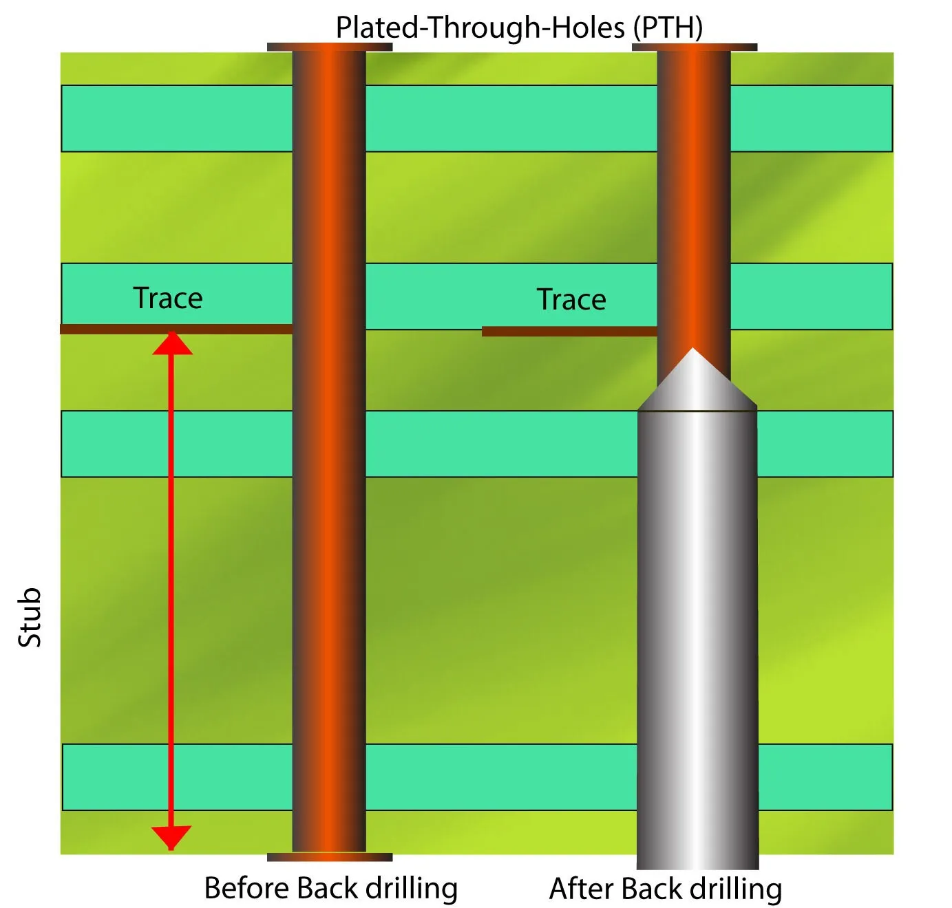
Controlled depth drilling, also known as back drilling, involves mechanically drilling into a plated through-hole via from one or both sides to remove the unused portion of the via barrel, or stub. This process uses a larger diameter drill bit than the original via to ensure clean removal while avoiding damage to the functional interconnect. Depth control relies on precise programming of the drilling machine, often monitored through peck drilling cycles that clear debris and maintain accuracy. The result is a shortened via that minimizes electrical length, reducing parasitic inductance and capacitance effects critical in high-frequency signals. Factory processes emphasize aspect ratios and drill exit locations to prevent breakout or misalignment during plating. This method aligns with manufacturing standards that specify tolerances for via geometry and plating integrity.
In practice, controlled depth drilling proves particularly valuable for thick boards where through vias would otherwise create long stubs. Engineers specify target depths based on layer stackup, ensuring the stub ends above the landing layer. Post-drilling inspection verifies depth via cross-section analysis or electrical testing. While it adds a processing step, the technique avoids the need for sequential lamination required in more advanced via structures. Depth tolerances typically demand sub-0.2 mm precision to preserve signal paths. Overall, it offers a practical upgrade for existing designs without full redesign.
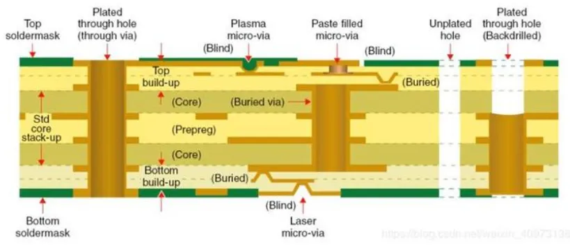
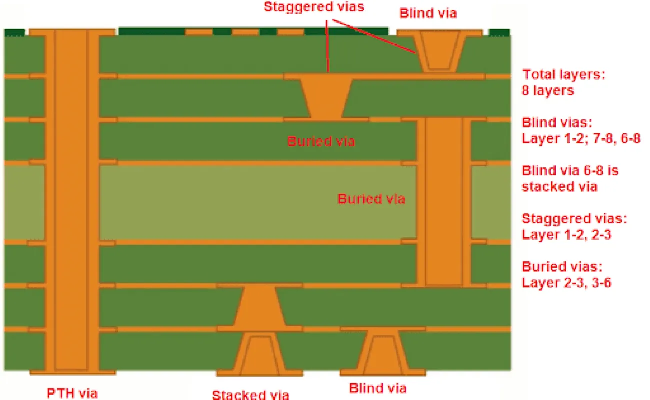
Overview of Blind Vias, Buried Vias, and Through-Hole Vias
Blind vias connect an outer layer to one or more inner layers without penetrating the full board thickness, achieved through sequential build-up or laser drilling for microvias. These vias eliminate stubs on the non-connected side, providing cleaner signal paths for HDI PCBs. Manufacturing involves lamination after partial drilling, followed by plating and filling in some cases. Buried vias, by contrast, interconnect only inner layers, invisible from the surfaces, and demand even more lamination cycles for their creation. Through-hole vias traverse the entire board, simplest to fabricate but prone to long stubs that act as antennas in high-speed applications.
Each type suits different scenarios: through-holes for low-cost, low-speed boards; blind vias for surface-to-inner routing in dense designs; buried vias for internal plane connections. Controlled depth drilling vs blind vias highlights a key distinction: back drilling modifies existing through vias post-plating, while blind vias require upfront stackup planning. Back drilling vs buried vias shows similar patterns, with back drilling offering stub reduction without added layers. These choices impact routing density and layer count significantly.
PCB Via Technology Comparison
A structured PCB via technology comparison reveals trade-offs across key metrics. Through-hole vias excel in cost and ease of fabrication but suffer from stub-related signal degradation above 1 GHz. Blind and buried vias provide superior density and signal integrity through shorter paths but increase manufacturing steps, lamination cycles, and yield risks. Controlled depth drilling bridges this gap by retrofitting through vias, achieving stub lengths comparable to blind vias at lower cost.
- Through-Hole: Signal integrity — Poor (long stubs); Routing density — Low; Manufacturing cost — Lowest; Complexity — Simple.
- Blind Via: Signal integrity — Good; Routing density — High; Manufacturing cost — High; Complexity — High.
- Buried Via: Signal integrity — Excellent; Routing density — Highest; Manufacturing cost — Highest; Complexity — Very high.
- Controlled Depth Drilling: Signal integrity — Good (reduced stubs); Routing density — Medium; Manufacturing cost — Moderate; Complexity — Moderate.
This comparison underscores high-speed PCB design choices: for frequencies up to 10 GHz, controlled depth drilling often suffices without HDI premiums. Cost-effective via solutions favor back drilling for mid-range multilayer boards, avoiding the expense of blind or buried vias unless density demands it. Factory yield data supports this, as back drilling leverages standard through-hole processes with one additional drill-pass.
Signal Integrity Considerations in High-Speed PCB Design
High-speed signals demand vias with minimal discontinuities to maintain impedance control and reduce insertion loss. Via stubs create resonant cavities that reflect energy, especially when stub length exceeds one-tenth of the signal wavelength. Controlled depth drilling addresses this by targeting stub removal to under 0.5 mm, aligning with design guidelines in IPC-2221 for printed board design. Blind vias inherently avoid full-depth stubs, ideal for RF transitions, while buried vias optimize inner-layer routing without surface interference.
Crosstalk arises from capacitive and inductive coupling between adjacent vias; shorter effective lengths from back drilling or blind structures mitigate this. Engineers model these effects using field solvers to predict return loss and eye diagrams. In stackups exceeding 1.6 mm thickness, back drilling proves essential for data rates above 5 Gbps. Pairing with ground stitching vias further shields signals. Standards like IPC-6012 emphasize plating uniformity post-drilling to ensure low resistance paths.
Manufacturing and Cost Implications
Manufacturing controlled depth drilling integrates into standard multilayer flows after through-hole plating, using specialized spindles for depth sensing. Tolerances challenge factories, requiring robust fixturing to prevent drill wander or breakout. Blind and buried vias necessitate sequential lamination, doubling or tripling press cycles, which escalates lead times and costs by 50-100% over through-holes. Back drilling vs buried vias favors the former for volumes under 1000 units, as it skips core removal steps.
Cost-effective via solutions prioritize through vias with back drilling for most applications, reserving blind/buried for HDI boards design. Panel utilization drops with complex vias due to alignment yields, amplifying per-unit expenses. Engineers optimize by grouping back-drill targets and specifying annular ring clearances. J-STD-001 provides assembly guidelines ensuring drilled vias withstand soldering stresses. Prototyping validates choices before production scale-up.
Best Practices for Via Selection and Implementation
Select via types based on stackup thickness, frequency, and density: use back drilling for boards over 1.6 mm with moderate pin counts. Specify drill depths with landing layer references in fabrication drawings. For controlled depth drilling vs blind vias, opt for back drilling if cost trumps ultimate density. Maintain back-drill diameters 10-20% larger than original vias for annular ring integrity.
In high-speed PCB design choices, simulate via stubs pre-layout to quantify improvements. Cluster vias for efficient drilling patterns, minimizing setup changes. Inspect depths via automated optical or X-ray methods per IPC-A-600 acceptability criteria. Cost-effective via solutions include hybrid approaches: buried for critical nets, back-drilled for others. Collaborate with fabricators early on capabilities.
Conclusion
Controlled depth drilling offers a compelling alternative in the spectrum of via techniques, balancing signal integrity gains with manufacturing practicality. Compared to blind and buried vias, it delivers cost-effective via solutions for high-speed PCB design choices without excessive complexity. Through-hole vias remain foundational, enhanced by back drilling where stubs pose risks. A thorough PCB via technology comparison guides engineers to optimal paths, ensuring performance aligns with project constraints. Adhering to standards fortifies reliability across production.
FAQs
Q1: What is the main difference between controlled depth drilling and blind vias?
A1: Controlled depth drilling modifies plated through-hole vias by removing stubs from one or both ends, preserving the interconnect while shortening electrical length. Blind vias connect surface to inner layers without full penetration, formed via sequential lamination or laser methods. Back drilling suits retrofits on standard multilayers, while blind vias enable higher density but at greater cost. This makes controlled depth drilling vs blind vias a key consideration for high-speed PCB design choices balancing budget and performance. Factory processes often favor back drilling for better yields within standard flows.
Q2: How does back drilling compare to buried vias in terms of cost and performance?
A2: Back drilling provides stub reduction on through vias at moderate cost, avoiding the multiple lamination cycles needed for buried vias that interconnect only inner layers. Buried vias offer superior signal integrity and density for internal routing but increase expenses significantly. Back drilling vs buried vias highlights cost-effective via solutions for mid-range boards, with comparable crosstalk reduction in many cases. Performance typically edges to buried vias for extreme frequencies, but back drilling suffices for most applications under IPC guidelines.
Q3: When should engineers choose controlled depth drilling in PCB via technology comparison?
A3: Opt for controlled depth drilling in thick stackups where through-via stubs exceed signal wavelength tolerances, prioritizing high-speed integrity without HDI premiums. It outperforms plain through-holes in reflections while undercutting blind vias in cost. Use PCB via technology comparison metrics like density, yield, and stackup constraints to decide. It is ideal for data rates to around 10 Gbps on 8–20 layer boards. Verify fabricator depth control capabilities and tolerances upfront.
Q4: What are practical tips for cost-effective via solutions using these techniques?
A4: Group back-drill sites to streamline programming, specify clearances per standards, and simulate stubs to confirm necessity. Use hybrid approaches—buried for critical nets, back-drilled elsewhere—to optimize budgets. Avoid over-specifying blind vias unless density or escape routing mandates them. Leverage standard processes for through vias enhanced by back drilling, and collaborate early with fabricators to align on capabilities and yield.
References
IPC-2221B — Generic Standard on Printed Board Design. IPC, 2012
IPC-6012E — Qualification and Performance Specification for Rigid Printed Boards. IPC, 2015
IPC-A-600K — Acceptability of Printed Boards. IPC, 2020


