










PCB Vias: Critical Design Factors for Manufacturing Yield and Reliability
What This Video Covers
Vias may appear simple in your PCB layout software, but they significantly influence fabrication cost, assembly success, and long-term product reliability. This video reveals practical via design guidelines that separate high-yield boards from problematic ones.
The content covers the risks of overusing tiny vias, which increase drilling complexity, tooling costs, and reduce structural integrity over time. It explains the critical importance of respecting aspect ratio — especially on thicker boards — to ensure consistent plating and prevent thin copper walls that lead to failures. Viewers learn the proper handling of via-in-pad designs, including filling and capping requirements to avoid solder wicking and weak joints during SMT assembly.
Additional emphasis is placed on standardizing drill sizes to streamline production and control costs. These manufacturability principles apply to rigid PCB, HDI PCB, multilayer PCB, and high-frequency designs.
Whether developing PCB prototypes or scaling to mass production, thoughtful via decisions made early prevent costly revisions and improve overall board performance.
Get an instant PCB quote or explore HDI PCB capabilities and turnkey PCB assembly services.
Key Highlights
- Via Size Matters: Avoid overusing tiny vias as they raise fabrication costs, complicate drilling, and reduce long-term mechanical reliability.
- Aspect Ratio Control: Maintain proper aspect ratio to ensure consistent plating; violations on thick boards lead to thin copper walls and field failures.
- Via-in-Pad Risks: Without filling and capping, vias in pads cause solder wicking, weak joints, and assembly defects.
Understanding Via Impact on PCB Fabrication and Assembly
PCB vias serve as essential interconnects in multilayer designs, but their configuration directly affects drilling, plating, and assembly processes. Poor via decisions can lead to higher scrap rates, extended lead times, and field failures under thermal or mechanical stress. Manufacturers prioritize designs that balance electrical performance with production efficiency.
In high-volume production, via parameters influence panel utilization, tool wear, and plating bath consistency. Engineers must consider the full fabrication sequence — from drilling to surface finish — to minimize defects such as voids, breakout, or incomplete plating.
Optimal Via Size Selection and Drill Standardization
Standardizing drill sizes across a design significantly improves manufacturing efficiency. Using multiple unique drill diameters requires additional tool changes, increases setup time, and raises the risk of registration errors. Preferred drill sizes (commonly 0.2 mm to 0.4 mm finished hole) allow fabricators to optimize stack drilling and maintain higher yields.
Overly small vias demand slower drilling speeds and more precise equipment, elevating costs and reducing throughput. Larger, standardized vias support better plating uniformity and mechanical strength while lowering overall board pricing.
Table: Recommended Via Sizes and Applications
| Via Type | Finished Hole Size | Typical Use Case | Manufacturing Benefit |
|---|---|---|---|
| Standard Through | 0.3–0.4 mm | Multilayer interconnects | High yield, cost-effective plating |
| Small Signal | 0.15–0.25 mm | High-density routing | Requires careful aspect ratio control |
| Via-in-Pad | 0.2–0.3 mm | BGA/CSP packages | Needs filling/capping for assembly |
| Thermal Relief | 0.25–0.5 mm | Power/ground planes | Improved heat dissipation |
Aspect Ratio Guidelines for Reliable Plating
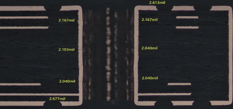
Aspect ratio — the ratio of board thickness to drill diameter — is a primary determinant of plating quality. Ratios exceeding 10:1 often result in uneven copper deposition, with thinner walls at the center of the hole. This creates reliability risks including barrel cracking during thermal cycling.
For standard 1.6 mm boards, designers should target aspect ratios of 6:1 or better for reliable plating. Thicker boards or HDI constructions require even stricter controls. Fabricators may apply specialized processes like pulse plating for challenging ratios, but these increase costs. Early DFM review helps identify and mitigate these issues.
Via-in-Pad Design Challenges and Best Practices
Via-in-pad constructions enable dense component placement but introduce significant assembly risks if not properly treated. Unfilled vias allow solder to wick away from the pad during reflow, resulting in insufficient solder volume and weak joints.
Recommended solutions include via filling with conductive or non-conductive epoxy followed by capping and planarization. This ensures a flat, reliable soldering surface. For high-reliability applications, filled and capped vias also improve thermal performance and reduce void formation.
Common Via-Related Manufacturing Failures and Prevention Strategies
Typical failures include plating voids from poor aspect ratio, drill wander on small holes causing breakout, and solder wicking in untreated via-in-pad designs. These issues often appear during ICT, functional testing, or accelerated life testing.
Prevention starts with comprehensive DFM analysis that verifies via parameters against fabricator capabilities. Collaboration with the manufacturer during the design phase allows for optimized stack-ups and material selection that support the intended via configuration.
Practical Recommendations for Multilayer and HDI Designs
In HDI boards, microvias and stacked vias demand precise laser drilling and sequential lamination processes. Designers should limit via stacking depth and maintain consistent dielectric thicknesses. For high-frequency applications, via stub length and back-drilling considerations become critical to signal integrity.
Always validate designs against the target manufacturer's capabilities chart. Standardizing via types and sizes across product families simplifies supply chain management and reduces qualification efforts for aerospace, medical, and industrial projects.
FAQs
Q1: Why do small vias increase PCB manufacturing costs?
A1: Tiny vias require smaller drills, more precise processes, and higher tooling costs while reducing yield and long-term reliability.
Q2: What is the risk of via-in-pad without proper treatment?
A2: Solder can wick into the hole during assembly, weakening solder joints, causing defects, and leading to reliability issues.
Q3: Why is standardizing drill sizes important in PCB design?
A3: Multiple drill sizes slow production, increase setup costs, and reduce overall manufacturing efficiency. Standardization improves yield and lowers pricing.
Q4: How does aspect ratio affect via reliability in thick PCBs?
A4: High aspect ratios make uniform copper plating difficult, often resulting in thin barrel walls prone to cracking under thermal stress. Designers should target ratios of 8:1 or lower for reliable performance in multilayer boards.
Q5: When should via filling and capping be specified?
A5: Via filling and capping are essential for via-in-pad designs, high-density BGAs, and applications requiring excellent thermal or mechanical performance. They also help maintain planarity for automated assembly processes.
Vias Look Innocent on screen?
But in real life, they control cost, reliability, and yield.
Here are some must-know tips.
One. Don't overuse tiny vias.
Smaller isn't always better.
Tiny drills increase fabrication complexity,
raise tooling cost,
and reduce structural reliability over time.
Two. Respect aspect ratio.
When the board is thick and the hole is narrow,
plating becomes inconsistent.
Thin copper walls are where long-term failures begin.
Three. Be careful with via-in-pad.
Without proper filling and capping,
solder can wick into the hole,
weakening joints and creating assembly defects.
Four. Standardize drill sizes.
Too many drill variations slow production and increase cost.
Good hole design isn't about routing freedom.
It's about manufacturability and controlled risk.





