 00:58
00:58
Signal Integrity
Signal integrity refers to the preservation of electrical signal quality as it travels through a circuit, ensuring minimal distortion, noise, or timing errors. In high-speed PCB design and electronics, maintaining signal integrity is crucial to prevent issues such as reflections, crosstalk, electromagnetic interference, and signal attenuation that can degrade system performance or cause failures. Engineers and designers often encounter these challenges in applications like data communication systems, automotive electronics, and consumer devices, where even minor signal degradation can lead to unreliable operation or data corruption. This tag page gathers resources focused on signal integrity principles, offering practical guidance for optimizing PCB layouts, selecting appropriate materials, and implementing effective mitigation strategies. For instance, you will find discussions on impedance matching techniques to reduce reflections, proper grounding methods to minimize noise, and simulation tools for predicting signal behavior before prototyping. These insights are particularly valuable for professionals troubleshooting real-world problems or students learning the fundamentals of high-frequency design, helping to bridge theoretical knowledge with hands-on application. By addressing common pitfalls and best practices, the content under the Signal Integrity tag equips you with actionable steps to enhance circuit reliability and efficiency. Whether you are designing for gigabit speeds or ensuring compliance with industry standards, these articles provide in-depth analysis and case studies that can inform your projects. Delving into these topics can refine your approach to electronics design, ultimately leading to more robust and performant systems.
Video Guide
-
00:58
-
 00:53
00:53
What is PCB Edge Plating? Benefits, Design Tips & Manufacturing Considerations
-
 00:52
00:52
How Many PCB Layers Do Beginners Actually Need?
-
 00:52
00:52
Stitching Vias in PCB Design: Essential for EMI Reduction, Heat Management & Signal Integrity
-
 01:09
01:09
How Signals Jump Between PCB Layers: Vias Explained
Technical Articles
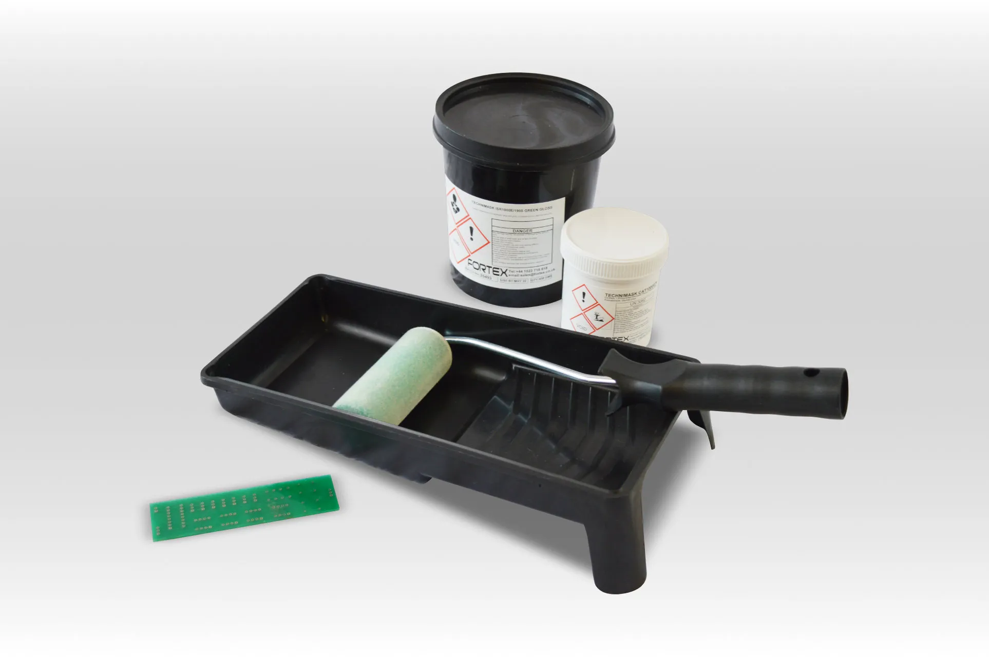
Liquid Photoimageable Resist for PCB Pattern Transfer: Process, Controls, and Practical Tips

PCB CAM Case Study on Tight Tolerances in Backdrilling, Countersink, and Press-Fit Holes

Press-Fit PCB Hole Design Standards and Process Best Practices
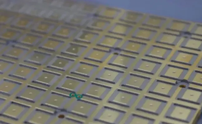
Technical Guide to 18-Layer Mixed-Lamination PCB
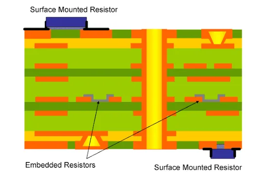
20-Layer Embedded-Resistor PCB: Process Flow and Core Manufacturing Challenges
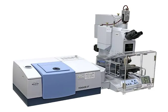
What Is FT-IR Spectroscopy and How Is It Applied in SMT Process Analysis?
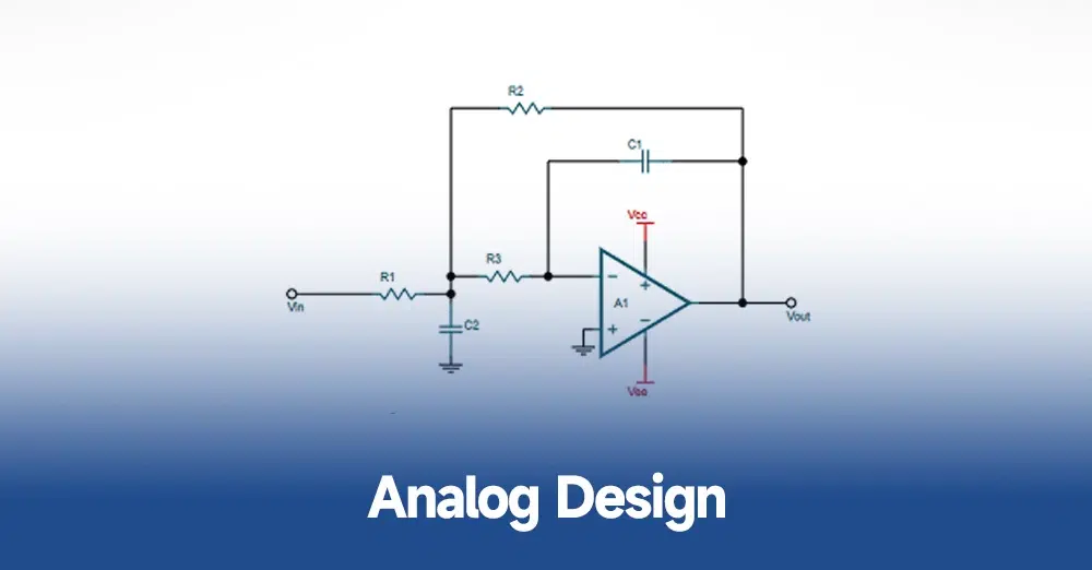
The Nine Stages of Analog Circuit Design

Understanding Ground in Electronic Circuits: Digital Ground vs. Analog Ground
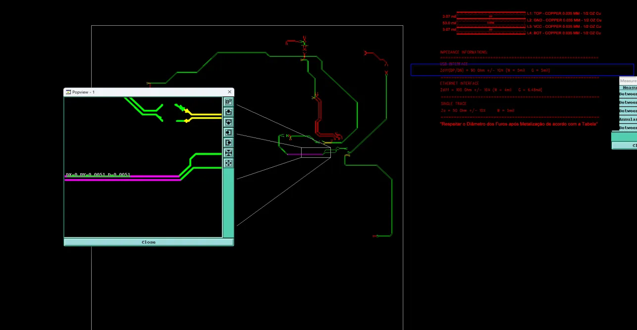
How PCB CAM Resolves Conflicting Impedance Control Requirements
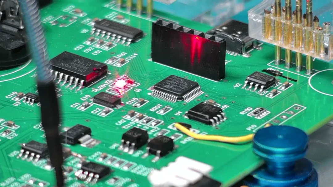
Output Waveform Analysis of a PWM Current-Control Circuit

PCB Layout and Routing Requirements for USB 2.0, USB 3.0, and USB Type C Interfaces

Should You Use Solid or Hatched Copper Pour on PCBs?
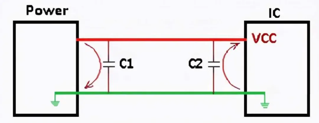
Why Two Capacitors? The Engineering Roles of 0.1 μF and 0.01 μF on the Power Rail

Why Do Eye Diagrams Collapse Even When High-Speed Interface Traces Are Length-Matched?
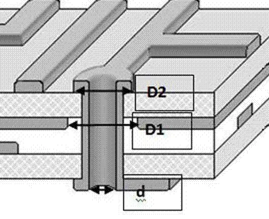
Why High-Speed PCB Traces Should Not Use Too Many Vias
ESD Isolated Conductors: Definition and Measurement for SMT Engineers

Nine Practical Rules for EMI Control in High-Speed PCB Design
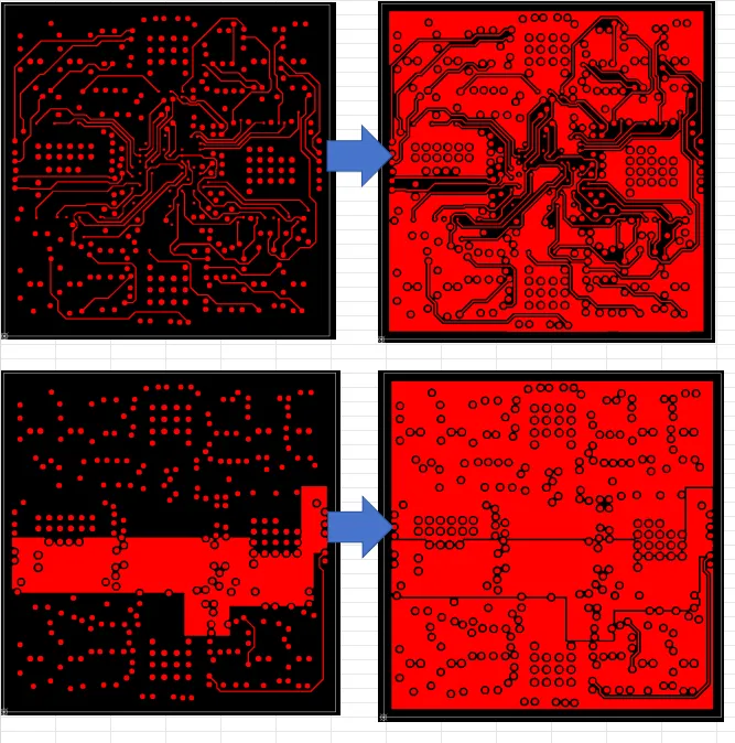
13 Common PCB Design Mistakes—and How to Avoid Them
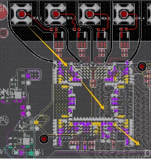
Mixed-Signal PCB Layout and Routing Design