High-speed PCB traces are not just “wires”; they are transmission lines whose electromagnetic fields interact with the surrounding dielectric and reference planes. In most multilayer printed circuit boards, two fundamental transmission-line structures are used to route signals: microstrip and stripline. Understanding how they are constructed, how their fields propagate, and how they differ in impedance control, electromagnetic interference (EMI), loss, and crosstalk is essential to reliable signal integrity and robust electromagnetic compatibility.
Microstrip
A microstrip is a surface-layer trace routed over a continuous reference plane (usually ground). The trace sits on the PCB dielectric, and its upper side faces air. In other words, one side of the field sees the PCB substrate and the other side sees air. The trace is typically covered by solder mask in production boards, but solder mask is much thinner and has a lower effective impact on fields than the bulk dielectric underneath.
Because a portion of the electric field lines extend into air (which has a dielectric constant close to 1), microstrip's effective dielectric constant is lower than that of the PCB substrate itself. This has two implications. First, for the same geometry, microstrip traces propagate signals faster than striplines. Second, the impedance of a microstrip depends on both the board dielectric and the air above, and small variations in solder mask and local environment can slightly influence impedance.
Microstrip's exposure to air also means some energy can radiate, and external fields can couple more readily into the trace. As a result, microstrip is generally more susceptible to EMI and can contribute more to radiated emissions compared to stripline, especially when return paths are poorly controlled. With proper stackup design, continuous reference planes, and disciplined routing (for example, avoiding plane splits and providing stitching vias near transitions), microstrip can still deliver excellent signal integrity with high bandwidth.
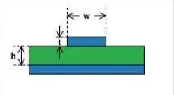
Figure 2-23 | Microstrip schematic
Stripline
A stripline is an internal-layer trace embedded between two reference planes. In a conventional symmetric stripline, the trace is centered between two planes at equal distances. In a double stripline configuration, two signal layers are placed between planes, each referenced to the same planes above and below. In both cases, the fields are predominantly contained within the dielectric between the planes, with minimal fringing into air since the trace is buried.
Because the electromagnetic fields are fully contained in the dielectric, stripline is well shielded. It exhibits lower radiation and is less susceptible to external noise pickup compared to microstrip. However, the effective dielectric constant for stripline is higher than microstrip (because the field is fully inside the dielectric), so signal propagation is slower. For the same impedance target, stripline typically requires different geometry than microstrip, often using narrower traces for the same dielectric thickness or adjusting the spacing to the planes.
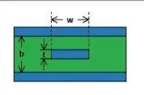
Figure 2-24 | Stripline schematic
Propagation Speed and Effective Dielectric Constant
The fundamental reason microstrip signals propagate faster than stripline signals is the difference in effective dielectric constant. Signal velocity v in a transmission line relates to the speed of light c and the effective dielectric constant εeff by v = c / √εeff. For a stripline, the field is fully within the substrate, so εeff is approximately the substrate's dielectric constant. For a microstrip, the field splits between air and substrate, yielding an εeff lower than the substrate's dielectric constant. Therefore, microstrip lines propagate faster. This affects timing, skew, and delay matching, particularly in wide buses and high-speed differential pairs distributed across both microstrip and stripline layers.
EMI, Radiation, and Susceptibility
Because microstrip fields fringe into air, they can radiate more readily, and they are more sensitive to nearby aggressors (for example, switching power nodes, long parallel traces, or external fields). By contrast, stripline's fields are largely confined between planes, reducing both emissions and susceptibility. For EMI-sensitive designs—such as RF sections, precision clocking, or interfaces subject to regulatory radiated-emission limits—stripline often provides a margin advantage.
That said, good microstrip design can manage EMI effectively. Key practices include maintaining continuous reference planes, avoiding plane splits under the trace, routing short return paths, adding stitching vias near layer transitions, and placing gaps to isolate noisy areas. Coplanar microstrip with ground pours (grounded coplanar waveguide) can further reduce fringing and improve impedance control while providing practical routing flexibility on outer layers.
Impedance Control and Stackup Considerations
Controlled impedance depends on geometry and materials. For both microstrip and stripline, the principal variables are trace width, copper thickness, distance to reference plane(s), and the dielectric constant of the substrate. For microstrip, since some field resides in air, solder mask thickness and dielectric constant also have a measurable, though smaller, influence on impedance. Removing solder mask over very high-speed outer-layer traces can slightly increase impedance and reduce variation, but this must be balanced against corrosion protection and manufacturability.
Stripline impedance is highly sensitive to the spacing between the signal layer and its reference planes. Symmetric stripline stackups help control impedance and reduce warpage, while consistent dielectric thickness and material uniformity are critical to keep impedance within tolerance. Because stripline is fully embedded, its impedance tends to be less affected by environmental factors than microstrip, making it attractive for tight-tolerance interfaces.
Irrespective of structure, impedance targets should be verified using field solvers or impedance calculators aligned with the specific stackup, materials, and copper thickness provided by the PCB fabricator. Communication with the fabricator to lock down the stackup and impedance tolerances early in the design reduces rework and improves yield.
Crosstalk and Coupling
Crosstalk depends on how much field lines from one trace couple to adjacent traces and nearby structures. For microstrip, fringing fields into air can increase lateral coupling, particularly when traces run in parallel for long distances. Grounded coplanar microstrip can reduce this coupling by confining fields more tightly. Increasing spacing, staggering routes, and using different reference planes for orthogonal directions across layers help control crosstalk.
Stripline is more symmetric and its fields are enclosed, so far-field radiation is lower. However, aggressors above and below a stripline layer can couple vertically, especially if parallel runs exist on neighboring layers. Layer-to-layer orthogonal routing and maintaining adequate spacing both within a layer and across adjacent layers reduce coupling. For both structures, keeping critical nets short, minimizing long parallel runs, and using solid planes for continuous return paths significantly limit crosstalk.
Loss Mechanisms and Frequency Behavior
Transmission-line loss arises from conductor loss (including skin effect and surface roughness) and dielectric loss. Stripline's fields are entirely inside the dielectric, so dielectric loss contributes more prominently than in microstrip at the same frequency. Microstrip, with some field in air, can exhibit slightly lower dielectric loss, but at very high frequencies it may incur additional radiation loss if return paths are not well managed.
Conductor loss increases with frequency as current crowds toward the surface (skin effect). Copper surface roughness further adds loss at high frequencies, influencing both microstrip and stripline. Selecting appropriate materials, specifying copper roughness limits when necessary, and keeping routes as short as practical help maintain signal quality. For very high-speed links, material selection and stackup symmetry often dominate the choice between microstrip and stripline.
Differential Pairs on Microstrip and Stripline
Differential pairs rely on equal and opposite currents with well-controlled odd-mode impedance. On microstrip, the pair's fields partly reside in air, making the effective dielectric constant lower and the pair's velocity higher compared to stripline. The coupling between the two traces (and to the reference plane) determines differential impedance; spacing, height above the plane, and trace width must be set together. Coplanar ground pours can reduce common-mode radiation and stabilize impedance, though they may increase capacitance to ground.
On stripline, the symmetric environment confines fields, and the pair experiences consistent dielectric loading above and below. This typically yields better containment of common-mode energy and improved EMI performance. However, because the velocity is lower, designers must account for longer propagation delay when matching timing across different structures. Maintaining consistent geometry and careful via design for each member of the pair is essential in both structures to limit intra-pair skew.
Via Transitions and Return Path Continuity
Layer transitions introduce discontinuities if return currents cannot find short, low-inductance paths. For microstrip, when a signal changes layers or crosses a plane split, the return must detour; adding stitching vias near the transition point and avoiding splits beneath the route maintains a compact return path and reduces loop inductance. For stripline, transitions between internal layers referenced to the same pair of planes are generally smoother, but attention to anti-pad sizes, plane continuity, and via stub length is still required to minimize impedance discontinuity and reflections.
Choosing Between Microstrip and Stripline
Both structures are essential tools rather than competing options. Use microstrip when:
- Outer-layer routing reduces via count and simplifies fan-out.
- Short routes and careful reference control keep EMI manageable.
- Faster propagation helps meet timing without excessive length compensation.
Use stripline when:
- EMI/EMC constraints are tight and field containment is critical.
- Consistent impedance with tighter tolerance is required across long routes.
- Dense designs benefit from internal routing between solid planes with controlled crosstalk.
In practice, most multilayer designs use both: microstrip for short surface routes, breakouts, and local connections, and stripline for longer high-speed runs and noise-sensitive paths. The final choice depends on stackup, impedance tolerance, timing, EMC goals, manufacturability, and cost.
Practical Design Notes
- Confirm stackup with the fabricator early, including dielectric thickness, copper weights, and materials, to achieve the intended impedances for both microstrip and stripline.
- Keep continuous reference planes under microstrip routes and avoid plane splits. Provide stitching vias near layer transitions to maintain return path continuity.
- Account for solder mask effects on microstrip impedance. For very high-speed interfaces, consider controlled mask thickness or mask openings, balanced against reliability needs.
- Use field solvers to validate geometry. Simple calculators provide quick estimates, but solvers capture effective dielectric constant, copper thickness, and proximity effects more accurately.
- Balance performance and density. Stripline may allow tighter channel density between planes with better EMI behavior, while microstrip can simplify routing and reduce via stubs at the cost of higher EMI sensitivity.
Understanding the electromagnetic differences between microstrip and stripline enables informed tradeoffs in PCB design. With disciplined stackup planning, impedance control, and careful routing, both structures can deliver robust high-speed performance, each excelling in scenarios aligned with its field behavior and physical constraints.
SEO Title: Microstrip vs Stripline: Classification and Differences of PCB Signal Traces Meta Description: Learn the differences between microstrip and stripline in PCB design, including field distribution, impedance control, EMI, loss, crosstalk, and practical stackup considerations for high-speed signal integrity.