










What is PCB Edge Plating? Benefits, Design Tips & Manufacturing Considerations
WHAT THIS VIDEO COVERS
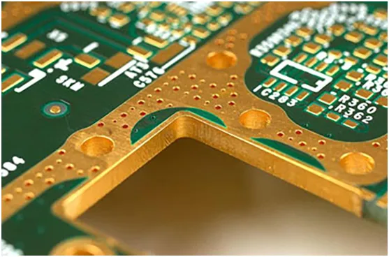
This video provides a clear explanation of PCB edge plating — a specialized technique where copper is plated along the edges of the board to electrically and mechanically connect the top and bottom layers. Often visible as a shiny metal "armor" around the perimeter, edge plating serves multiple critical functions beyond aesthetics.
It improves ground continuity, reduces electromagnetic interference (EMI), and prevents signal leakage near the board edges. Additionally, it enhances mechanical strength and aids in heat dissipation along the perimeter. The video highlights proper design considerations, routing rules, and the added manufacturing complexity involved.
Edge plating is particularly valuable in high-frequency PCB designs, RF antennas, connector-heavy boards, and applications requiring high reliability such as medical devices, aerospace, and industrial control systems.
The content emphasizes the importance of early discussion with your manufacturer, as edge plating affects PCB fabrication processes, plating specifications, and overall cost. Understanding this technique helps engineers make better decisions when balancing performance, reliability, and manufacturability.
KEY HIGHLIGHTS
- Edge Plating Function: Copper plating along board edges that electrically connects top and bottom layers while creating a continuous ground shield.
- Performance Benefits: Significantly reduces EMI, improves signal integrity near edges, and strengthens power/ground planes.
- Additional Advantages: Enhances mechanical durability and thermal dissipation, making it valuable for RF and high-reliability applications.
How PCB Edge Plating Works in Fabrication
PCB edge plating extends standard fabrication by milling the board edges before applying electroless and electrolytic copper deposition. This creates a continuous conductive layer along the perimeter that ties together top and bottom copper features, including ground planes. The process requires precise control during panelization, drilling, and plating to ensure uniform coverage without voids or thinning at corners.
In production, fabricators typically route slots or expose edges early in the workflow. Inner layers must maintain adequate pullback to prevent unintended shorts when edge copper is deposited. Poor adhesion can occur if edges are not properly cleaned and roughened prior to plating, leading to delamination under thermal stress or mechanical flex.
Real-world CAM reviews often flag edge plating specifications that conflict with V-cut or tab routing, requiring custom panelization adjustments. Early EQ (Engineering Question) communication with the manufacturer is essential to align on copper thickness, edge coverage percentage (typically full perimeter or specified segments), and compatibility with final routing tolerances.
Key Performance Benefits for High-Frequency and RF Designs
Edge plating forms a Faraday cage-like shield that confines EMI emissions and improves return paths for high-speed signals near board perimeters. This is critical in RF modules where edge radiation can degrade performance. It also bolsters power and ground plane integrity, reducing impedance discontinuities.
Thermally, the plated edge acts as an additional heat-spreading path, particularly beneficial for boards with high-power components or dense layouts. In multilayer constructions (6-12 layers), it helps mitigate warpage by balancing mechanical stresses around the perimeter.
Practical testing in manufacturing environments shows measurable reductions in radiated emissions and improved signal-to-noise ratios when edge plating is properly implemented alongside controlled impedance traces.
Critical DFM Guidelines and Routing Rules for Edge Plating
Designers must incorporate specific clearances: typically 0.25 mm or more between internal copper features and the plated edge to avoid shorts during depanelization. Routing keep-out zones around edges prevent trace damage, while fiducials and tooling holes need careful positioning away from plated areas.
Annular ring considerations extend to edge features, and teardrops may be recommended at connections to plated edges. For panels with multiple boards, stamp holes or mouse bites require coordination with edge plating boundaries to maintain structural integrity during separation.
Recommended Clearances for Edge Plating
| Parameter | Typical Value | Purpose | Common Issue if Violated |
|---|---|---|---|
| Copper to Edge Clearance | 0.25 mm (10 mil) min | Prevent shorts during routing | Copper chipping or bridging |
| Edge Plating to Cutout/Slot | 2.5 mm (100 mil) | Ensure uniform plating adhesion | Voids or uneven coverage |
| Inner Layer Pullback | 0.15-0.3 mm | Avoid layer shorts | Inter-layer electrical failure |
| Minimum Edge Coverage | Full perimeter or 80% | Consistent shielding/grounding | Inconsistent EMI performance |
Common Manufacturing Challenges and Failure Modes
Insufficient edge preparation can result in plating voids, particularly at corners or high-aspect areas, leading to unreliable ground connections and potential EMI leaks in the field. Uneven copper deposition may cause thickness variations that affect mechanical strength or create stress points during thermal cycling.
Depanelization of edge-plated boards demands modified routing strategies; aggressive scoring or incorrect tab placement can chip the plating, exposing base material to oxidation or corrosion over time. In high-volume production, these issues increase scrap rates and require additional inspection steps such as cross-sectioning.
To mitigate risks, specify plating thickness (typically matching or exceeding standard copper weight) and request pre-production samples for validation. Collaboration on stackup and material selection (e.g., FR-4 vs. high-Tg) further reduces warpage risks associated with added edge copper.
When to Specify Edge Plating: Applications and Alternatives
Edge plating excels in RF antennas, high-speed digital boards with edge connectors, medical imaging equipment, and aerospace systems where EMI containment and ruggedness are paramount. It also benefits dense IoT modules exposed to vibration or thermal extremes.
Note on Alternatives: Edge plating differs from castellated (plated half-holes), which are discrete interconnect features for board-to-board soldering rather than continuous shielding. For applications needing only localized connections, castellated holes may offer a more cost-effective solution.
Cost and Lead Time Implications in Production
Edge plating introduces additional milling, plating baths, and inspection steps, typically increasing costs by 20-50% and extending lead times depending on panel utilization and volume. Early design-for-manufacturability reviews help optimize specifications to control expenses while achieving required performance.
FAQ
Q1: When should you use edge plating on a PCB?
A1: Edge plating is recommended for RF and high-frequency designs, boards with connectors near edges, or applications sensitive to EMI. It's also useful when extra mechanical strength or improved heat spreading is required.
Q2: Does edge plating increase PCB manufacturing cost?
A2: Yes. Edge plating adds process steps and requires precise control during fabrication and plating, increasing both cost and lead time. Always confirm capabilities with your manufacturer early in the design phase.
Q3: What are the main design challenges with PCB edge plating?
A3: Designers must carefully manage keep-out zones, routing clearance, and plating specifications. Poor implementation can cause plating voids, uneven coverage, or issues during lamination and drilling.
Q4: How does edge plating differ from castellated holes?
A4: Edge plating provides continuous copper along the full board perimeter for shielding and grounding. Castellated holes are individual half-plated vias on the edge primarily for board-to-board soldering and modular assembly. Each serves distinct electrical and mechanical purposes; mixing them requires specific DFM coordination.
Q5: What clearance rules are critical for reliable edge plating?
A5: Maintain at least 0.25 mm between internal copper and the board edge, with greater spacing around slots or cutouts. Inner layer pullback prevents shorts, and proper tab routing during panelization avoids damage to the plated edge. Violating these can lead to field failures from EMI leakage or mechanical weakness.
Ever seen a PCB with shiny metal wrapping around its edges?
That's not decoration — it's a clever design trick called edge plating.
Edge plating means copper is plated along the sides of the board,connecting the top and bottom layers — like giving your PCB a metal armor.
Without it, signals near the edge can leak noise,and the ground may lose continuity — causing EMI or instability.
With edge plating, the board gains more than just protection.
It helps block EMI, keeps signals clean, and strengthens the ground.
The metal frame also boosts mechanical strength and even improves heat dissipation along the edges.
Designers use it in RF boards, antennas, or connector zones,but it needs careful routing and plating precision.
Edge plating usually means a more complex process —so always confirm the requirements with your manufacturer first.
This is aivon, making pcb learning easier,hope this help,Comment below — and follow for more PCB tips!





