 02:22
Board Edge Spacing
Board edge spacing is a critical aspect of printed circuit board (PCB) design that refers to the minimum distance required between components, traces, vias, and the outer edges of the board. This parameter ensures mechanical stability, protects against physical damage during manufacturing and assembly, and complies with industry standards such as IPC-7351. For engineers and designers searching for information on board edge spacing, understanding these guidelines can prevent common issues like edge chipping, solder mask delamination, or interference with enclosures and mounting hardware. In practical applications, proper board edge spacing enhances PCB reliability by accommodating depanelization processes, such as V-scoring or routing, without compromising signal integrity or thermal performance. For instance, maintaining at least 0.5 mm clearance from traces to the board edge reduces the risk of shorts during handling, while larger spacings may be necessary for high-voltage designs to meet creepage and clearance requirements. Best practices include consulting fabrication capabilities early in the design phase, using CAD tools to automate spacing checks, and incorporating fiducials near edges for precise alignment in automated assembly lines. Neglecting these can lead to increased production costs or failures in field deployment. Articles tagged with Board Edge Spacing provide in-depth guidance on optimizing these distances for various board types, from rigid to flexible PCBs. By reviewing these resources, you can apply proven strategies to your projects, ensuring robust designs that balance functionality with manufacturability. Whether you are troubleshooting a prototype or scaling up for production, these insights help refine your approach to achieve higher yields and longer product lifespans.
Video Guide

Technical Articles
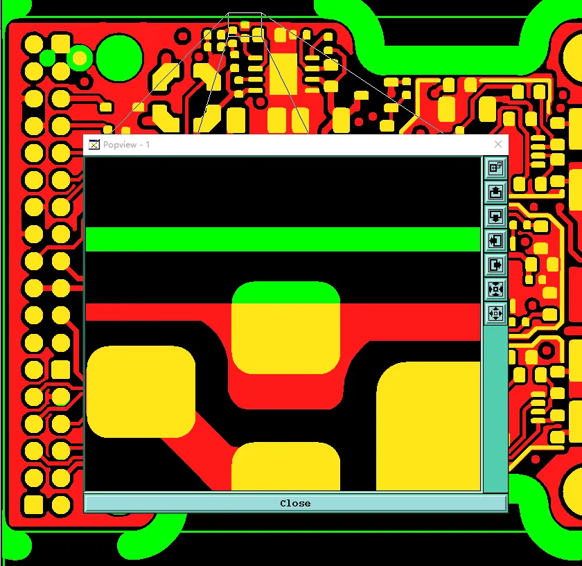
PCB CAM Review for Copper and SMD Pads Near the Board Edge

Why Components Must Be Kept Away from PCB Edges: Understanding SMT Rail Keep-Out Zones
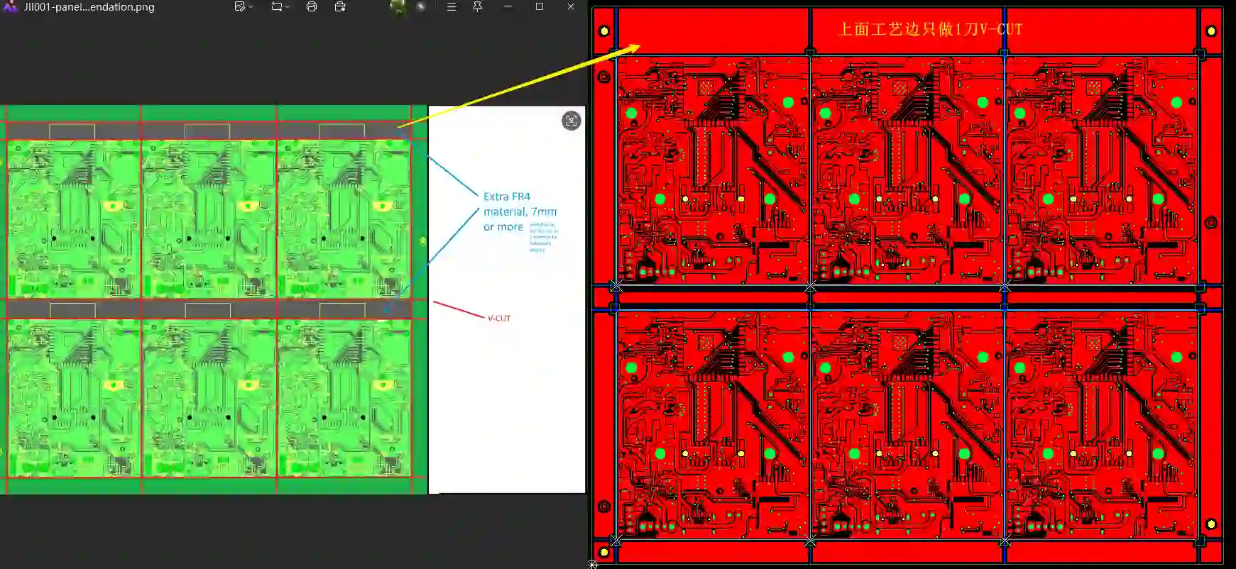
How to Solve 2-Layer PCB CAM Issues Before Manufacturing
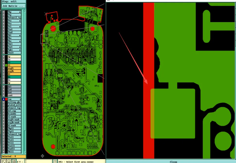
Engineering Case Study: 4-Layer 1.0mm FR-4 PCB Edge Clearance and Stamp Hole Spacing DFM Review
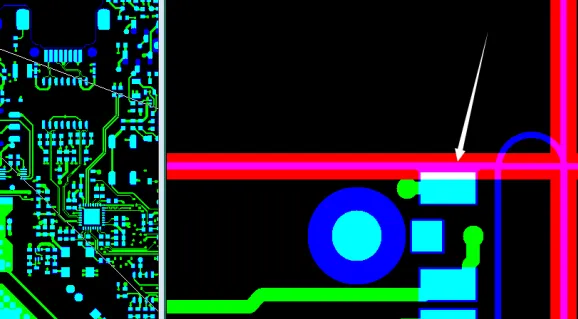
4-Layer FR-4 PCB CAM Review Case: Addressing Via Tenting Conflicts, Routing Layer Discrepancies, and V-CUT Edge Clearance Risks
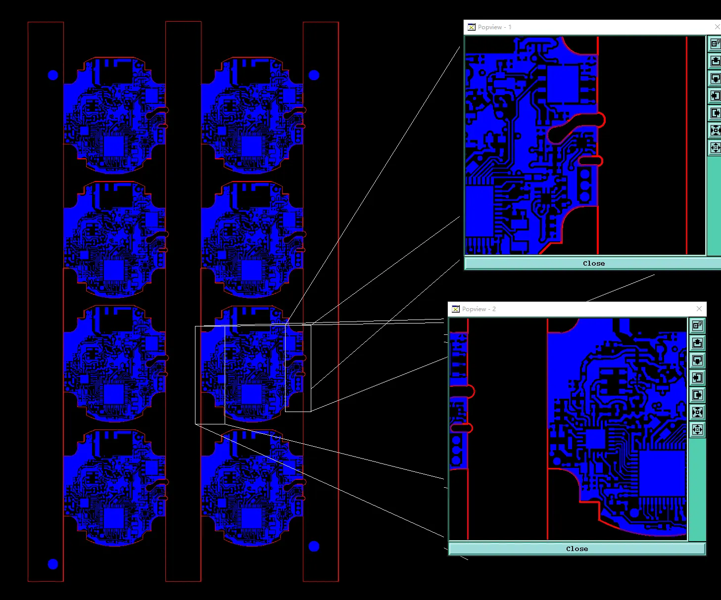
Trace to Board Edge Clearance: Essential DFM Rules
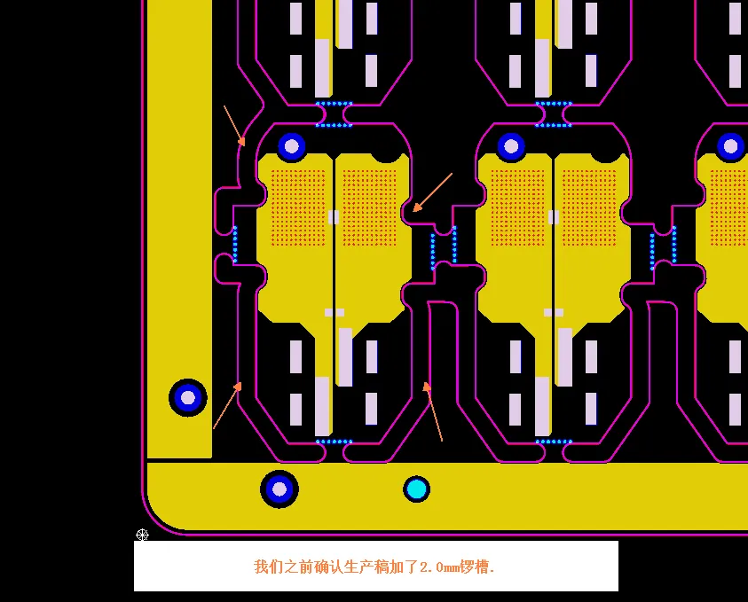
PCB Panelization Slot Design: Why Your Gerber Needs Routing Paths
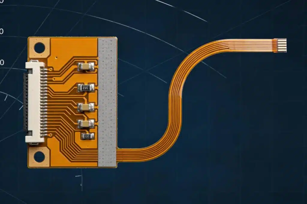
How Much Clearance Between FPC Trace and Board Edge Is Safe?
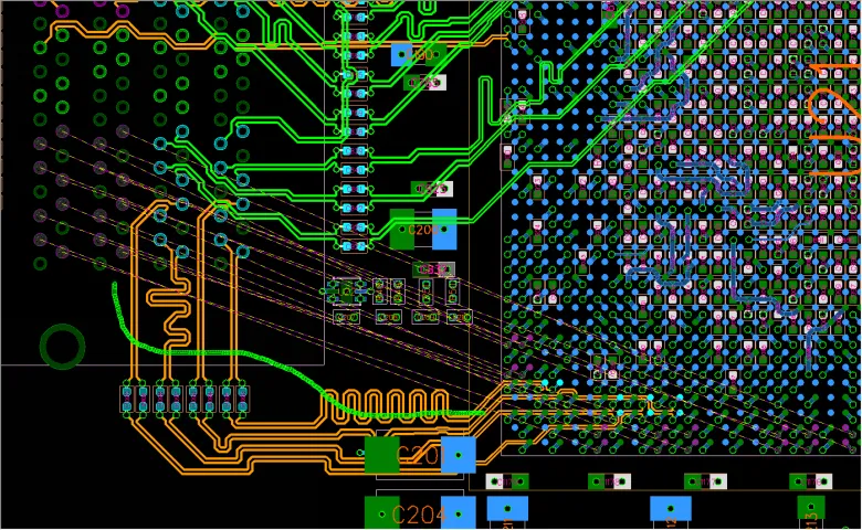
Basic Design Rules for hobbyists
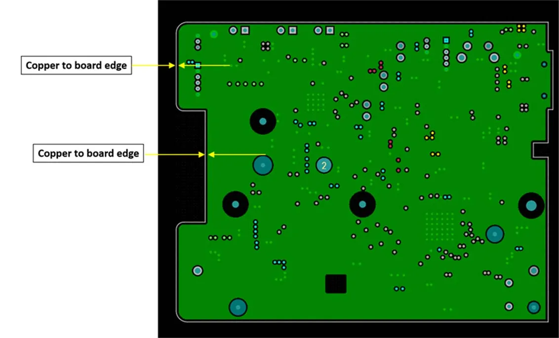
FR4 PCB Edge Clearance: How Much Copper Should Be Kept from the Board Edge?
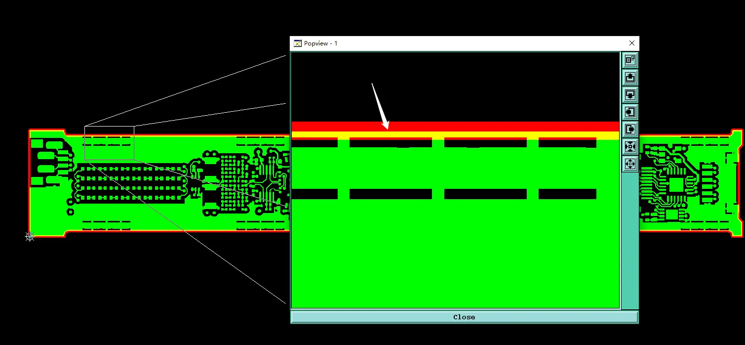
Preventing Exposed Copper from Copper to Outline Clearance Issues