Medium-sized 4-layer FR-4 boards with 0.5oz copper and tight feature-to-edge spacing commonly require significant DFM adjustments during CAM review. This case examines a 143.5 × 196 mm board. During engineering analysis, multiple critical issues involving copper-to-outline clearance and stamp hole design were identified, necessitating customer confirmation to prevent edge defects and mechanical failures.
As a senior CAM engineer, I have reviewed numerous designs where edge proximity issues lead to production problems. In this order, several locations showed copper and holes too close to the final outline, along with stamp hole spacing concerns, triggering targeted Engineering Questions (EQs).
Order Overview
This 4-layer FR-4 board ( #FR4-20260311-037 ) featured TG150 material, 1.0mm finished thickness, and 0.5oz copper on inner and outer layers. The design specified ENIG surface finish, 0.3mm minimum hole size, green solder mask, white silkscreen, and 6mil line width/spacing. Production involved 100% flying probe testing, customer panelization (3x2), V-scoring with routing, and mechanical forming. Quantity was 30 pieces.
The relatively thin profile for a 4-layer board and customer panelization made edge protection and mechanical feature optimization particularly important.
Main Engineering Questions Found During CAM Review
1. Multiple Copper-to-Outline and Hole-to-Edge Clearance Issues
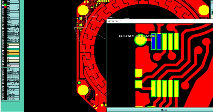
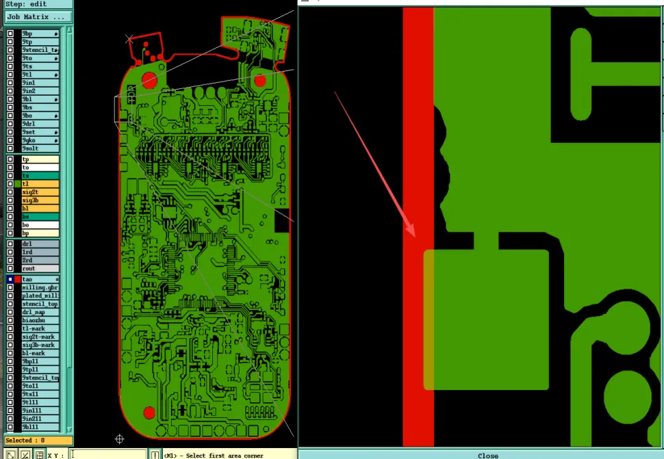
Several areas showed copper features and non-plated holes positioned extremely close to the final board outline (as tight as 1.17mil in one location). Pads were also found extending beyond the outline in some spots.
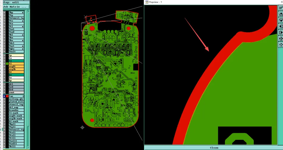
Figure 1: copper positioned close to the board outline
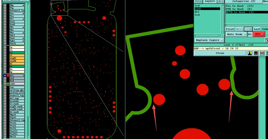
Figure 2: non-plated holes positioned extremely close to the final board outline

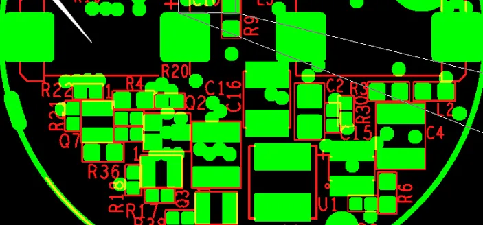
Figure 3: some pads were found extending beyond the outline
We noticed these violations during outline-to-copper and drill overlay analysis. Our engineer raised EQs because insufficient clearance risks exposed copper, burrs, and copper peeling after routing or V-scoring. On a 1.0mm board with 0.5oz copper, these issues are particularly prone to causing edge defects.
If ignored, the boards could suffer from edge short circuits, copper peeling during handling, or cosmetic defects that fail inspection. In worst cases, this leads to scrap or field failures due to exposed copper corrosion. According to IPC-2221 spacing guidelines, adequate clearance from copper to edge is essential for reliability.
2. Stamp Hole Spacing Too Tight for Reliable Depanelization
The stamp holes (mouse bites) had 0.2mm spacing, which is too tight for stable depanelization. Additionally, some stamp hole sizes were inconsistent, and holes near process edges needed verification for deletion.
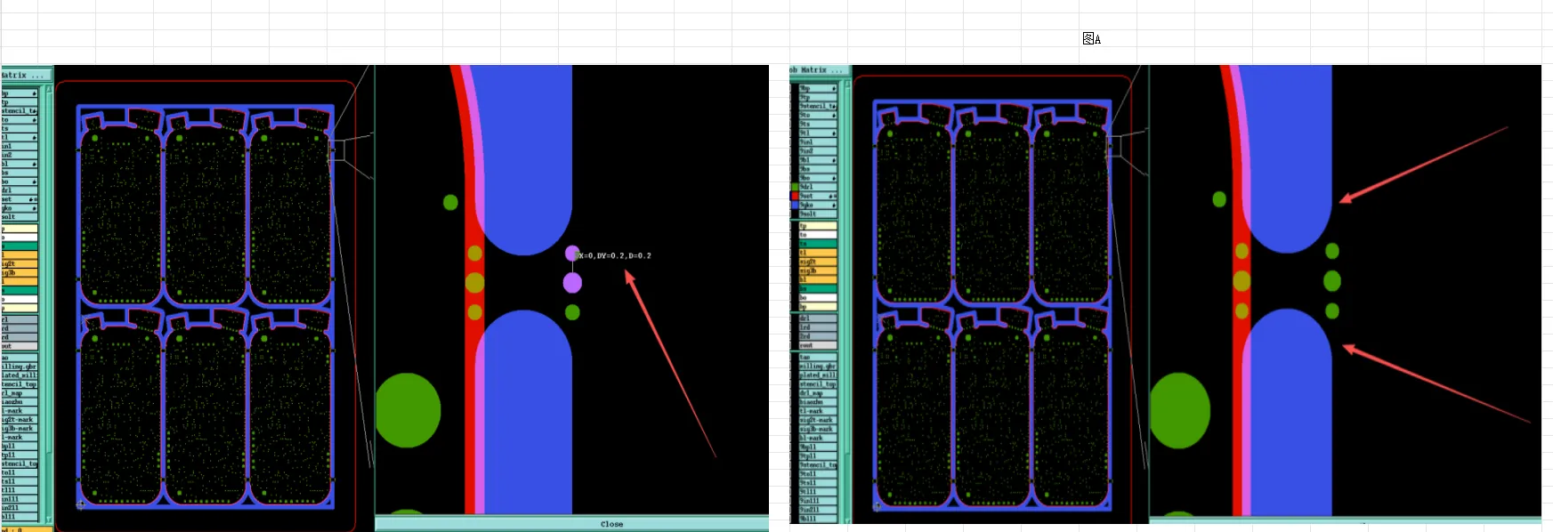
Figure 4: stamp holes had 0.2mm spacing, which is too tight for stable depanelization
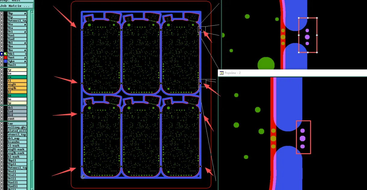
Figure 5: stamp holes near process edges
Our CAM team identified this during mechanical layer review. We suggested adjusting spacing to 0.35mm and standardizing hole size to 0.4mm to prevent premature breaking or rough edges. We also proposed deleting stamp holes too close to process edges.
If left unchanged, the tight spacing could cause boards to break during panel handling or leave jagged edges, leading to assembly difficulties and cosmetic defects. Inconsistent stamp holes increase the risk of uneven stress during depanelization.
3. Process Edge Copper Pour and 0.5mm Hole Clarification
To improve plating uniformity and help control potential board warpage on this 1.0mm 4-layer panel, our team proposed adding copper pour on the process edges. We noticed that many thin multilayer boards benefit from this technique during electroplating, as it balances current distribution and reduces the risk of uneven copper thickness or panel bowing.
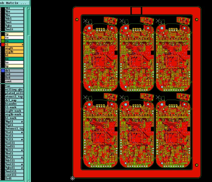
Figure 6: copper pour on the process edges
Separately, a 0.5mm hole on the bottom layer had a smaller solder mask opening. We raised an EQ asking whether this was intended as a plated via or a plug-in hole, because the tight mask opening could allow solder mask ink to enter the hole during application, potentially causing plating defects or assembly issues.
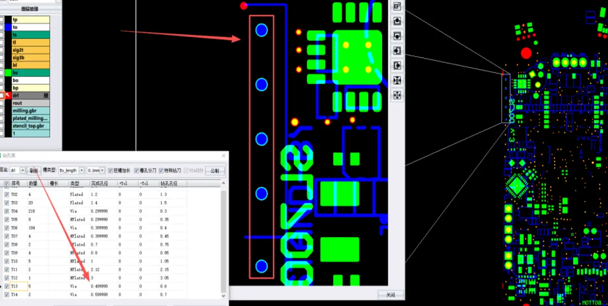
Figure 7: a 0.5mm hole on the bottom layer had a smaller solder mask opening
Our CAM engineer confirmed these points after reviewing the drill, mask, and mechanical layers. The process edge copper suggestion was a proactive DFM recommendation based on our experience with similar panelized orders. If the 0.5mm hole clarification had been ignored, ink intrusion could lead to incomplete plating or blocked holes, resulting in open circuits or poor solderability.
The customer approved the process edge copper pour for better quality and confirmed the hole type, allowing us to finalize the production files. These adjustments helped ensure reliable fabrication and reduced overall manufacturing risk for this order.
Manufacturing Risks and DFM Insights
Edge clearance violations are among the most common DFM issues on panelized boards. Designers frequently place features too close to the outline without considering routing tolerances. Stamp hole spacing below 0.35mm often causes premature separation or rough edges.
Ignoring these could lead to exposed copper, burrs, copper peeling, and assembly problems. On 0.5oz copper boards, such defects increase scrap risk and signal issues in final products.
How the Engineering Team Resolved the Issues
Our team provided detailed screenshots with measurements and suggested specific clearance increases and stamp hole adjustments. The customer approved the process edge copper pour for better plating quality. Hole types and mask openings were clarified, allowing accurate CAM programming.
We noticed the edge issues early and optimized the files after confirmation. This proactive approach protected yield on this panelized order.
Final Manufacturing Outcome
All EQs were resolved with customer approval. Clearances were increased, stamp holes standardized, and production files updated. The order was released for fabrication with optimized parameters.
Key Takeaways for PCB Designers
- Maintain sufficient copper and hole clearance to board outline (typically >0.3mm) to prevent exposed copper and edge defects.
- Design stamp holes with 0.35mm+ spacing and consistent size for reliable depanelization.
- Consider adding copper pour on process edges for improved plating uniformity and reduced warpage on thin boards.
- Clearly specify hole types (plated vs non-plated) and mask opening requirements.
- Review all mechanical features against final outline in Gerber data.
- Account for 0.5oz copper etching tolerances in fine feature designs.
- Confirm acceptance of any process recommendations like edge copper.
- Perform edge clearance checks before submitting panelized designs.
FAQ
Q1: Why is copper-to-outline clearance important?
A1: Insufficient clearance causes exposed copper after routing, leading to shorts, peeling, burrs, or corrosion, especially on panelized boards.
Q2: What spacing is recommended for stamp holes?
A2: Minimum 0.35mm spacing with consistent 0.4mm hole size ensures clean depanelization without premature breaking or jagged edges.
Q3: Should process edges include copper pour?
A3: Yes, it improves plating uniformity and helps control board warpage, particularly beneficial for thin multilayer panels.
Q4: What happens if pads extend beyond the board outline?
A4: It leads to exposed copper, copper peeling, and potential short circuits at the board edge after depanelization.