PCB Specifications
| Parameter | Value | Parameter | Value |
|---|---|---|---|
| PCB Type | FR4 PCB | Quantity | 5 pcs |
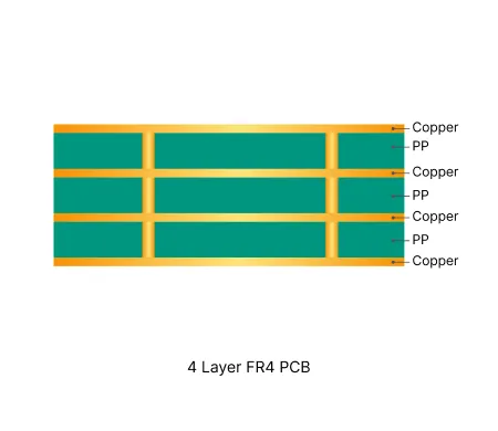
| Layers | 4 Layers | Board Type | Panel PCB |
| Dimensions | 143.5 x 196 mm | Copper Weight | 0.5oz |
| Thickness | 1 mm | Min Track / Spacing | 6/6mil↑ |
| Surface Finish | ENIG (Immersion Gold) | Min Hole Size | 0.3mm↑ |
| Solder Mask | Green | Silkscreen | White |
| Stack-up | Default | Impedance Control | No |
Manufacturing Timeline
Logistics Information
Key Manufacturing Processes
Manufacturing Summary
This 4-layer FR-4 board measured 143.5 × 196 mm with 0.5 oz copper on inner and outer layers and a 1.0 mm finished thickness using KB-6165F material. Produced in a quantity of 30 pieces as customer self-panelized 3×2 arrays with routing separation, the design featured standard 6 mil line/space, ENIG surface finish, and no process edges. 100% flying probe testing was performed with mechanical forming. The thin copper and multiple edge-related features required careful DFM attention.
Several clearance issues were identified during review. Copper features, pads, and non-plated holes sat too close to the board outline, risking edge exposure, burrs, and copper peeling after routing. Stamp hole spacing of 0.2 mm was below reliable thresholds and risked premature panel separation or breakage; adjustments to 0.35 mm spacing with consistent 0.4 mm holes were proposed and confirmed. A plug-in hole with smaller bottom window risked solder mask intrusion. Additional copper on process edges was requested for plating uniformity and warp control. These concerns were resolved through direct file adjustments and confirmations.
Production completed within the 10-day schedule with all parameters verified to specification. The panels maintained good flatness and registration despite the absence of process edges, delivering consistent boards suitable for customer assembly.
Explore More PCB Manufacturing Resources
4 Layer FR4 PCB Manufacturing Insights
Standard multilayer solution offering practical routing density and controlled impedance for industrial and consumer electronics.

Multilayer FR4 PCB Engineering Queries Explained: Causes, Risks and Solutions
In-depth guide to the most frequent Engineering Queries (EQ) and DFM issues in Multilayer FR4 PCB (4/6/8+ layers) production. Real factory insights on stack-up confirmation, impedance control, copper balance, inner layer design, via treatment, registration, and practical prevention strategies.
Real Production Records
| Order ID | PCB Type | Layers | Dimensions | Solder Mask | Surface Finish | Quantity | Action |
|---|---|---|---|---|---|---|---|
| FR4-20260520-046 | FR4 PCB | 2 | 94.21 x 275 | Green | ENIG (Immersion Gold) | 75 | View detail |
| FR4-20260515-068 | FR4 PCB | 14 | 244 x 267 | Green | ENIG (Immersion Gold) | 10 | View detail |
| FR4-20260506-017 | FR4 PCB | 6 | 55 x 41.7 | Green | ENIG (Immersion Gold) | 15 | View detail |


