










A six-layer FR-4 board measuring 107.25 mm by 16 mm arrived for production review with a target finished thickness near 0.89 mm, 1 oz copper on all layers, immersion gold finish, and green solder mask on both sides. The design was panelized as a 1x2 array using routing slots combined with stamp holes, process edges of 4 mm on all four sides, and a request for 100 percent flying-probe testing. From a DFM perspective, the primary concern was manufacturing stability of the board edge once mechanical routing began. Copper features sat unusually close to the outline, creating a clear risk that the finished edge would expose copper after the router cut. This case illustrates how a single clearance issue, if left unaddressed, can cascade into cosmetic rejects, reliability problems, and yield loss on an otherwise straightforward thin multilayer board.
The engineering review treated every observation as a potential production failure waiting to happen. Rather than asking whether the files could be fabricated, the team asked what would go wrong if fabrication proceeded without clarification. The answers shaped a set of preventive actions that protected both first-pass yield and long-term field reliability.
Copper to Outline Clearance That Triggered the First EQ
Our CAM engineer noticed that multiple copper features on outer and inner layers approached the board ( FR4-20260414-039 ) outline far more closely than standard process capability allows. On a thin 0.8–0.89 mm six-layer construction, the mechanical router that forms the final perimeter leaves a small but unavoidable kerf and positional tolerance. When copper sits inside that tolerance band, the finished edge can expose copper or leave a ragged copper remnant.
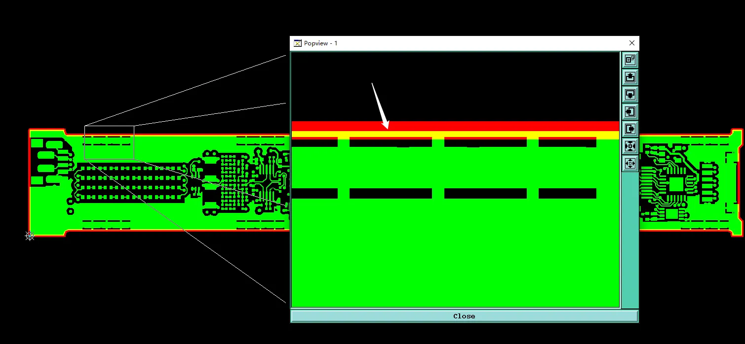
Figure 1: the copper on the board edge is too close to the outline
From a DFM perspective, the primary concern was manufacturing stability of the edge. Exposed copper after routing is more than a cosmetic defect. It creates a preferential path for oxidation, moisture ingress, and potential shorting against chassis or adjacent boards during assembly. On immersion-gold boards the exposed copper also appears as a visible discontinuity against the gold surface, raising the probability of customer rejection under IPC-A-600 edge-condition criteria.
The recommendation was straightforward and preventive: shave copper 8 mil inward from the centerline of the outline, except in the limited regions where plating edges were intentionally required. This single adjustment moved every copper feature safely outside the routing tolerance window while preserving the electrical connectivity the designer intended.
| Clearance Condition | Observed Distance | Risk After Routing | Recommended Action |
|---|---|---|---|
| Copper to outline (critical areas) | Below process capability | Exposed copper, oxidation, cosmetic reject | Shave 8 mil from outline centerline |
| Plating-edge exceptions | Intentional | Controlled exposure only | Leave unmodified |
| Remaining perimeter | Adequate after shave | Clean edge, full solder-mask coverage | Proceed to production |
Table 1. Copper-to-outline risk assessment used during DFM review. The 8 mil inward shave moved features outside the routing tolerance band and eliminated the dominant edge-exposure risk.
Panelization, Stamp Holes, and Tooling Marks on Process Edges
The customer specified a 1x2 array separated by routing slots and stamp holes. External Mark points that fell outside the individual boards were to be ignored. Process edges of 4 mm on all four sides were available for the addition of tooling holes and replacement fiducials.
From a DFM standpoint, the risk was not the panelization method itself but the potential loss of registration features. If external marks were simply deleted without adding new ones on the process edge, downstream assembly equipment would lack reliable fiducials. On a narrow 16 mm board the consequence would be misaligned placement or, in the worst case, boards rejected at the SMT line.
Our engineering team therefore confirmed that the external marks could be omitted and that tooling holes plus new Mark points would be added on the 4 mm process rails. The routing-slot spacing of 5.00 mm by 5.00 mm and the stamp-hole pattern remained unchanged. This approach preserved the customer's preferred depanelization method while restoring the registration accuracy required for reliable assembly.
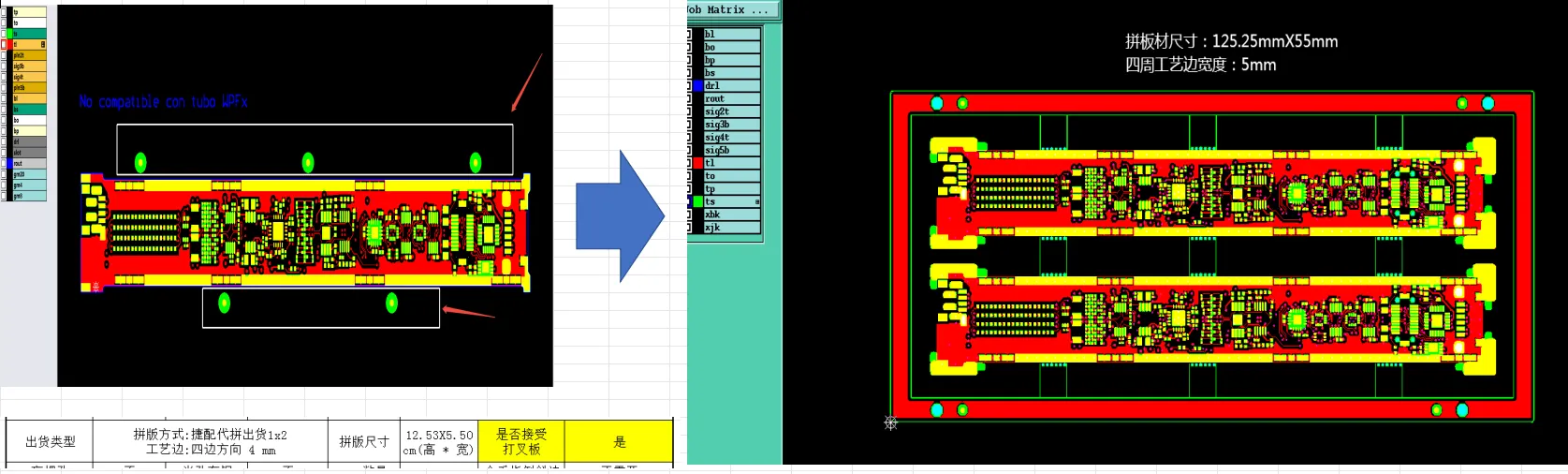
Figure 2: tooling holes and fiducial marks shall be added to the edge rail
Solder Mask Openings Between IC Pads and the Bridge Decision
A second visual check of the outer layers revealed numerous IC and discrete-pad openings that left only minimal solder-mask dams between adjacent pads. The original design intentionally opened the mask between many of these features. The EQ asked whether solder mask bridges should be forced or whether the openings should be left exactly as drawn.
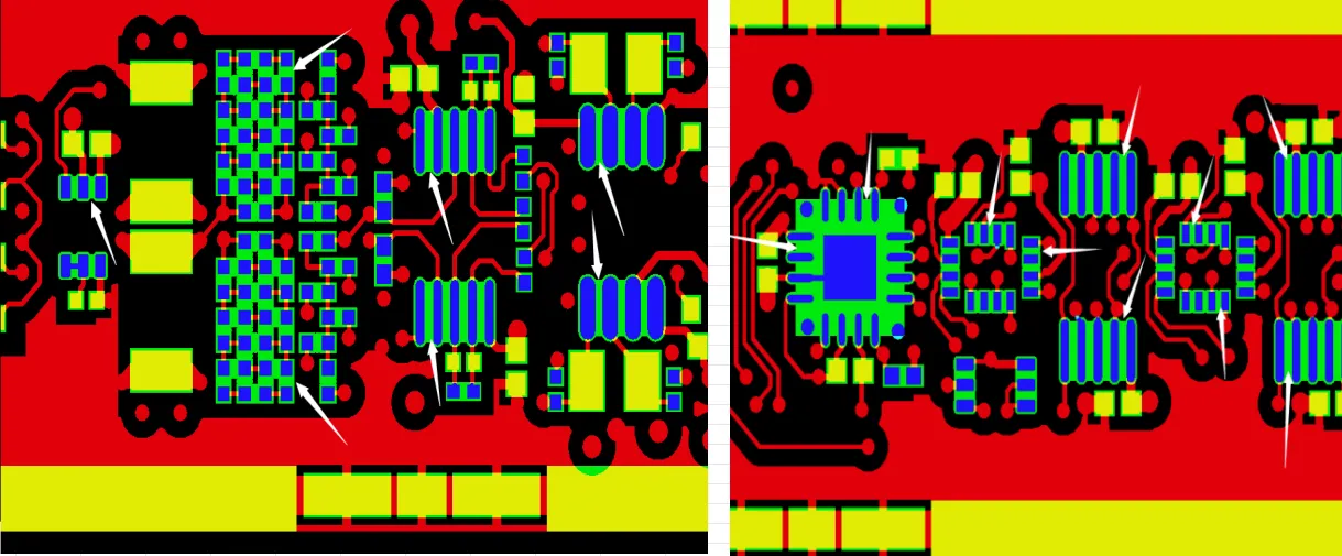
Figure 3: designs with solder mask openings between ICs and pads
The manufacturing risk of leaving the openings unchanged is solder bridging during reflow, especially on fine-pitch devices. Conversely, forcing bridges where the designer had deliberately removed them can create solder-mask residue on pad surfaces, degrading solderability. Because the board uses immersion gold and is intended for automated assembly, the safer path was to honor the original opening design while confirming that the customer understood the residual bridging risk.
The final instruction recorded in the EQ was therefore: "Solder mask openings shall be made the original design." This decision kept the design intent intact and placed the residual assembly risk under the customer's explicit control rather than introducing an unrequested process change.
| Design Feature | Original Intent | Potential Failure if Altered | DFM Decision |
|---|---|---|---|
| IC pad openings | Open mask between pads | Solder bridging or mask residue | Keep original openings |
| Solder-mask dams | Minimal or absent | Assembly shorts | Customer-confirmed risk acceptance |
Table 2. Solder-mask opening evaluation. Preserving the original design avoided introducing new solderability risks while documenting the residual bridging exposure for the customer.
Stackup Thickness and Finished Copper Confirmation
The fabrication notes requested a finished board thickness of 0.89 mm ± 0.1 mm with 1 oz finished copper on every layer. The order header had listed a nominal 0.8 mm, creating a minor but important discrepancy. On a six-layer construction this thin, even a 0.1 mm shift can affect impedance control (although impedance was not required), warpage behavior, and connector fit.
The engineering team therefore confirmed that the stackup would be built exactly to the attached drawing: finished copper 1 oz on all layers and overall thickness 0.89 mm ± 0.1 mm. Because the copper distribution was balanced and no resin-filled vias or heavy copper zones were present, the risk of excessive warpage remained low once thickness was locked.
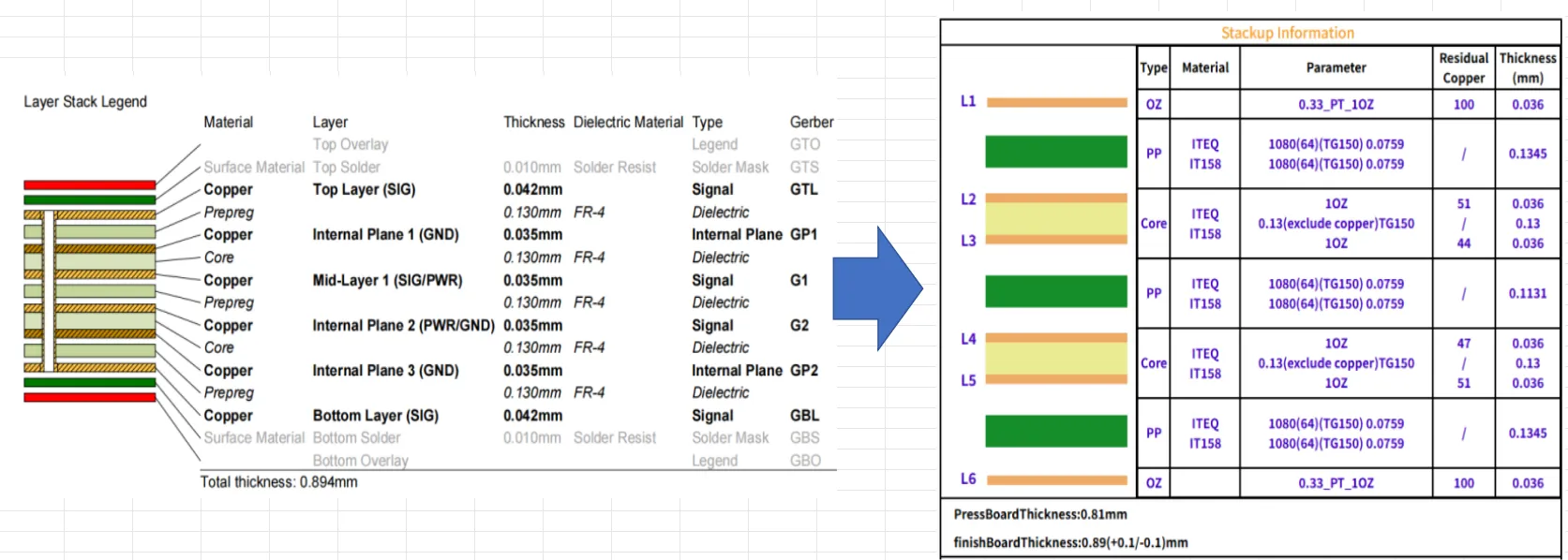
Figure 4: fabricate the stackup as shown in the attached drawing
A secondary observation concerned the GM4 designator layer. This layer existed solely to aid assembly and contained no copper or mask data required for the bare board. The decision to ignore GM4 for fabrication was therefore low-risk and simply removed an unnecessary processing step.
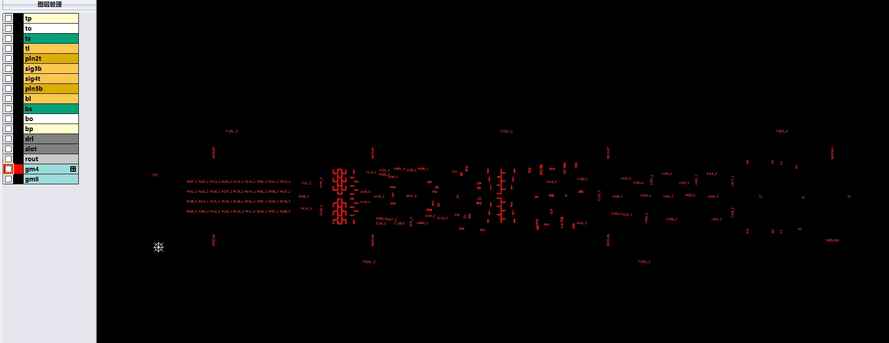
Figure 5: GM4 layer
Failure Scenarios the DFM Review Explicitly Prevented
If the copper-to-outline clearance had been left unchanged, mechanical routing would have produced boards with intermittent exposed copper along the perimeter. In subsequent handling and assembly those edges could have shorted against metal fixtures or neighboring boards, generated cosmetic rejects under visual inspection, and created long-term corrosion sites once the product entered the field. On an immersion-gold board the contrast between gold and exposed copper would have made the defect highly visible, elevating the scrap rate.
If external Mark points had been deleted without replacement tooling marks, the 1x2 panels would have reached the SMT line without reliable fiducials. Placement accuracy on the narrow 16 mm boards would have degraded, increasing the probability of tombstoning, misaligned components, and ultimately open or short circuits after reflow.
If solder-mask bridges had been forced against the original design intent, pad surfaces could have retained residual mask, reducing solder wetting on immersion gold and producing weak joints. Conversely, leaving the openings without customer confirmation would have left an undocumented bridging risk. Both outcomes were avoided by a single clarifying question.
These failure modes are realistic, not theoretical. They arise directly from the interaction of design geometry with the mechanical and chemical processes used to build a thin six-layer FR-4 board.
Preventive Actions Taken Before Production Release
The DFM team translated each observation into a concrete, low-impact change:
- Copper features were shaved 8 mil inward from the outline centerline, except where plating edges were required. This restored safe clearance without altering net connectivity.
- External Mark points were omitted as requested; new tooling holes and fiducials were added on the 4 mm process edges so that panel registration remained intact.
- Solder-mask openings between IC pads were fabricated exactly as drawn, preserving design intent while documenting residual assembly risk.
- The stackup was locked to the customer drawing: 1 oz finished copper on all layers and 0.89 mm ± 0.1 mm overall thickness.
- The GM4 designator layer was ignored for fabrication, eliminating an unnecessary process step.
Each recommendation was presented to the customer with the manufacturing evidence that supported it. Once confirmation was received, the files were released to production with the knowledge that the dominant edge-exposure, registration, and solderability risks had already been closed.
| Risk Category | If Ignored | After DFM Action |
|---|---|---|
| Edge copper exposure | Oxidation, shorts, scrap | Clean routed edge |
| Fiducial loss | Placement error | Tooling marks restored |
| Solder-mask residue or bridging | Assembly defects | Original openings preserved |
| Thickness mismatch | Warpage or fit issues | 0.89 mm locked |
Table 3. Before-versus-after risk summary. Each preventive action converted a high-probability manufacturing defect into a controlled, documented condition.
Building Trust Through Proactive DFM
This review demonstrates that the highest-value engineering work often occurs before the first panel is drilled. By identifying copper-to-outline clearance, registration-feature gaps, and solder-mask opening intent early, the team prevented defects that would otherwise have appeared only after routing, plating, or assembly. The customer received boards whose edges were free of exposed copper, whose panels carried the tooling features needed for accurate placement, and whose solder-mask openings matched the original design intent.
The same preventive logic applies to any thin multilayer design that pushes copper features close to the perimeter or relies on external marks for registration. Engaging DFM review at the file-submission stage remains the most reliable way to convert latent manufacturing risks into controlled, documented decisions before production begins.
FAQ
Q1: Why does insufficient copper to outline clearance create exposed copper after routing?
A1: Mechanical routers operate with a finite kerf width and positional tolerance. When copper features lie inside that tolerance band, the cutting tool can leave copper partially or fully exposed on the finished edge. On immersion-gold boards the contrast is highly visible and can lead to cosmetic rejects or long-term corrosion sites.
Q2: What manufacturing risk appears if external Mark points are deleted without replacement?
A2: Assembly equipment loses reliable fiducials. On narrow boards such as the 16 mm design in this case, placement accuracy degrades, increasing the probability of misaligned components, tombstoning, and post-reflow opens or shorts.
Q3: Why confirm solder-mask openings between IC pads rather than automatically adding bridges?
A3: Forcing bridges against the original design can leave residual mask on pad surfaces, reducing solder wetting on immersion gold. Leaving the openings without confirmation leaves an undocumented bridging risk. Explicit customer confirmation places the residual risk under controlled acceptance.
Q4: How does a 0.1 mm thickness discrepancy affect a thin six-layer board?
A4: Even a small shift can alter warpage behavior, connector fit, and overall mechanical stiffness. Locking the stackup to the drawing value of 0.89 mm ± 0.1 mm removes this variable before production begins.
Q5: Can a designator layer such as GM4 safely be ignored during fabrication?
A5: Yes, when the layer contains only assembly-aid information and no copper or mask data required for the bare board. Ignoring it eliminates an unnecessary process step without affecting electrical or mechanical performance.
Q6: What is the most effective way to prevent edge-exposure defects on thin multilayer boards?
A6: Perform a copper-to-outline clearance check against actual routing tolerance before release. A modest inward copper shave, typically 8 mil from the outline centerline, moves features outside the process window and eliminates the dominant source of exposed copper after mechanical routing.






