A 4-layer FR-4 board measuring 117.81 mm × 99.06 mm arrived for CAM review with customer-supplied panelization already defined as a 2 × 5 array. The order specified mechanical routing as the depanelization method, immersion gold finish, via tenting, and zero process edge. Quantity was limited to 20 pieces across two sets. At first glance the package appeared complete: Gerber files, a separate panel drawing, and a project PDF. Yet during data verification the mechanical layer, stamp-hole features, and the accompanying PDF failed to describe a single, unambiguous separation method. The resulting interpretation gap prevented release to production and forced a focused engineering investigation into the panelization slot design itself.
Customer Panel Intent Limited to Stamp Holes
The designer clearly intended a customer-defined panel that could be shipped intact and later separated by the assembly house. The Gerber mechanical data contained only stamp holes (mouse bites) along the board edges inside the 2 × 5 array. No continuous routing slots or milling gaps were present between the individual boards. At the same time the project PDF showed continuous routing slots, and the order parameters listed "routing" as the depanelization method together with a 2.00 mm × 2.00 mm routing spacing value. Board thickness was stated as 1.6 mm, copper weight 1 oz on all layers, TG150 material, and minimum finished hole 0.25 mm. Via tenting was required by the fabrication notes. The overall intent therefore appeared to be a low-cost, mechanically formed panel that relied on mouse bites for break-away while still referencing routing in the documentation.
This mixture of features created an immediate manufacturing-interpretation problem. Stamp-hole-only panels and routed-slot panels are processed with different tooling paths, different panel rigidity during plating, and different edge-quality expectations after separation. Without a single authoritative definition, the factory could not decide which process path to program.
Gerber Mechanical Layer Versus Project PDF Discrepancy
The first data cross-check compared the Gerber mechanical layer against the project PDF. The Gerber contained stamp holes exclusively; the PDF contained continuous routing channels. Further inspection of the customer-supplied panel drawing confirmed that no milling gap existed between the boards. The order ( #FR4-20260709-057 ) parameters, however, listed a 2.00 mm routing spacing, which is the factory's default minimum for safe routing-bit clearance on 1.6 mm FR-4. Our CAM engineer also noted that the panel carried zero process edge, leaving no sacrificial material outside the array. Under these conditions any misinterpretation of the separation method would transfer directly into the finished board outline.
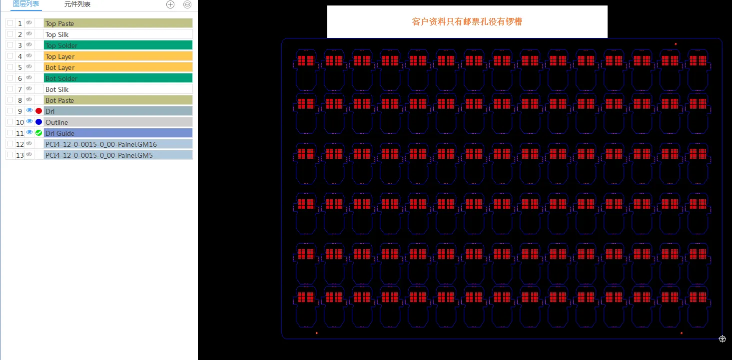
Figure 1: the Gerbe file only has stamp hole but no routing
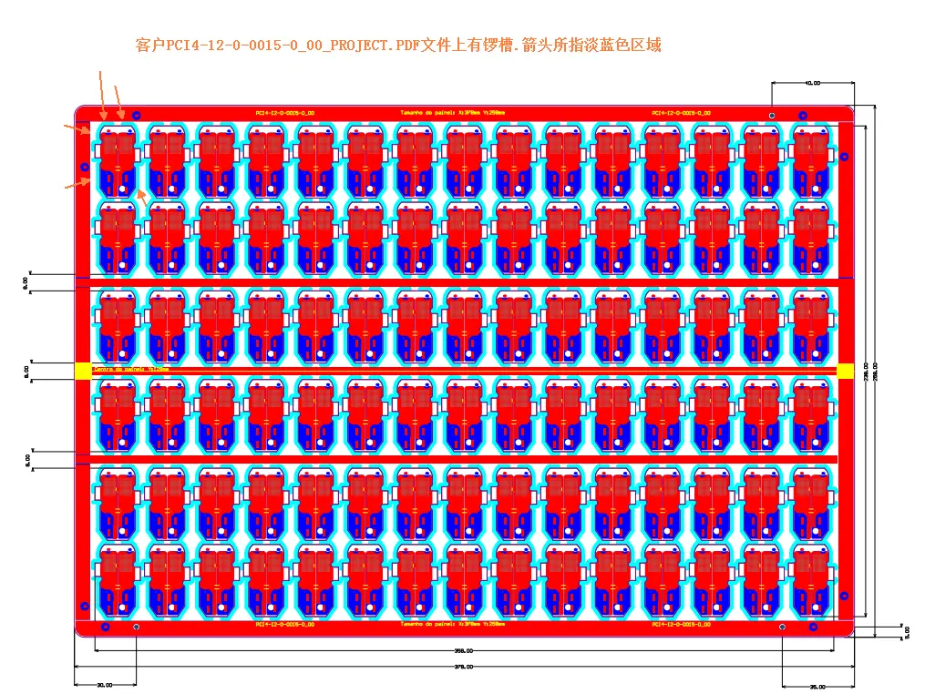
Figure 2: there are routing in PDF
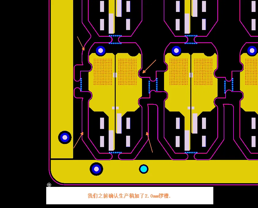
Figure 3: added the 2.0mm routing in the previous production file
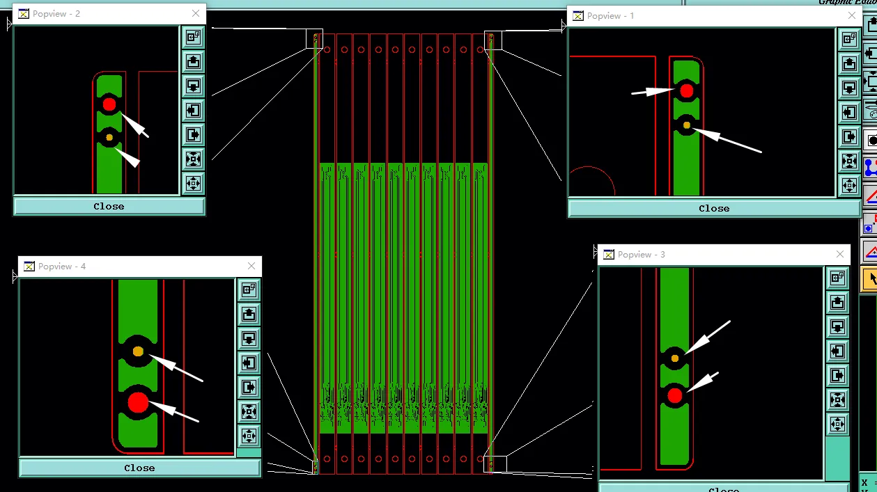
Secondary observations reinforced the primary concern. Several holes marked as plated-through (PTH) in the drill attributes lacked corresponding pads of adequate size or showed no electrical connection on the copper layers. Board thickness values appearing in different documents were not identical. Via openings in the solder-mask layers were drawn equal to the via diameter even though the fabrication notes required tenting. Each of these points raised its own clarification need, yet all of them were secondary to the panelization conflict: until the separation method was locked, the tooling and process sequence themselves remained undefined.
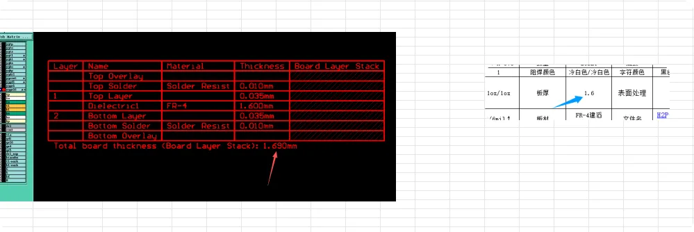
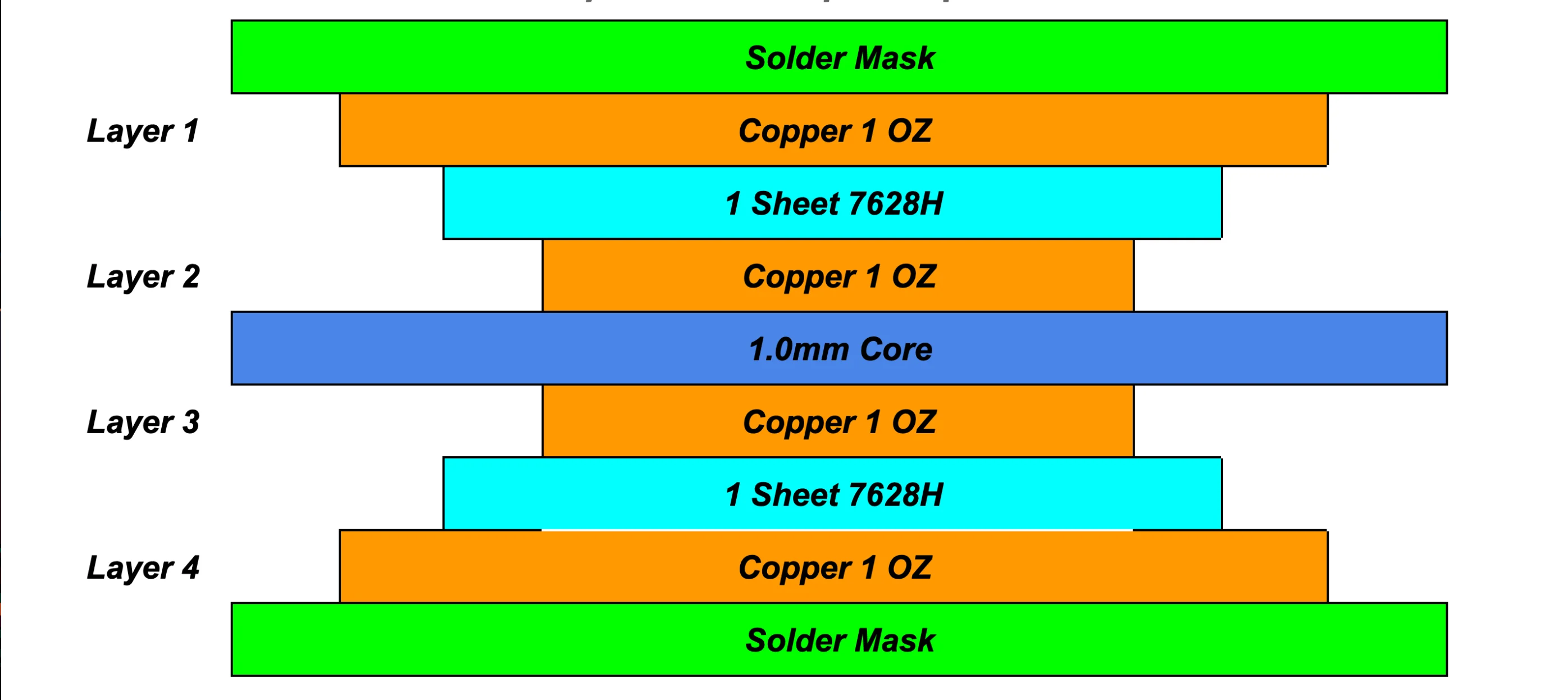
Figure 4: the board thickness is inconsistent
Panelization Slot Design Conflict Between Gerber and PDF
The dominant conflict belonged to the category of manufacturing-interpretation conflict combined with documentation inconsistency. Three independent sources described the panel separation method differently:
- Gerber mechanical layer and customer panel drawing – stamp holes only, no routing slots, no milling gap.
- Project PDF – continuous routing slots present.
- Order parameters – depanelization method listed as routing, spacing value 2.00 mm × 2.00 mm.
Because the panel was customer-supplied and carried zero process edge, the factory could not simply add features without confirmation. Adding a 2 mm routing slot would change the board outline by removing material that the Gerber did not authorize. Leaving the panel as stamp-hole only would ignore both the PDF and the order's routing designation, potentially producing an edge finish that the customer did not expect. IPC-A-600 Class 2 edge criteria still apply after depanelization; an uncontrolled fracture along stamp holes on a 1.6 mm laminate can leave residual fibers or uneven copper, while a properly routed slot yields a clean, dimensionally stable edge.
If production had proceeded on the stamp-hole-only data, two realistic manufacturing outcomes were possible. First, the panel might survive plating and shipping but fail at the customer's depanelization station because the stamp-hole strength and pitch were never validated against the expected break-away force. Second, if the factory had unilaterally inserted 2 mm routing slots to match the PDF, the finished boards would be undersized relative to the Gerber outline, risking dimensional rejection. Either path constituted an uncontrolled interpretation of design intent.
| Source Document | Separation Feature Shown | Milling Gap Present | Manufacturing Implication |
|---|---|---|---|
| Gerber Mechanical Layer | Stamp holes only | No | Break-away force undefined; edge quality after fracture unknown |
| Customer Panel Drawing | Stamp holes only | No | Zero process edge leaves no margin for added features |
| Project PDF | Continuous routing slots | Implied | Conflicts with Gerber outline dimensions |
| Order Parameters | Routing method listed | 2.00 mm stated | Factory default assumes milling gap exists |
The table above crystallized the conflict for the engineering team. Design intent could not be read with confidence from any single document; each source partially contradicted the others. Production release was therefore blocked until the customer confirmed which representation governed the final panelization slot design.
Supporting Issues: PTH Pad Size and Via Tenting Mismatch
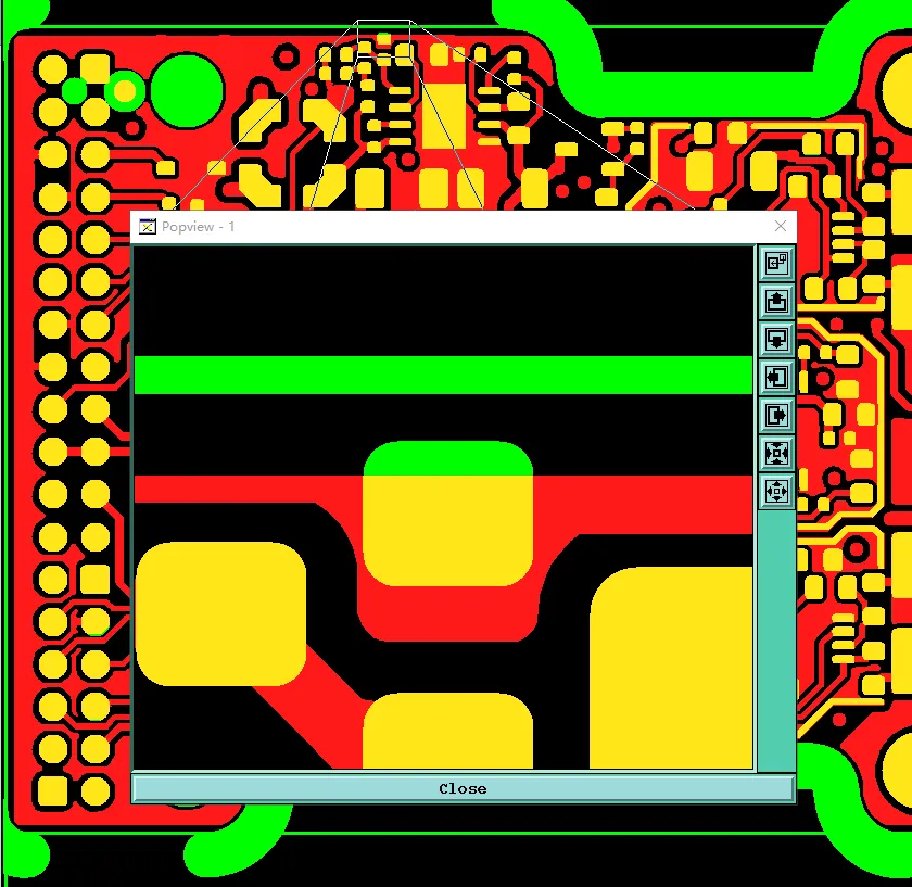
While the panelization conflict remained primary, three secondary observations were recorded because they could interact with the final process path. First, several holes attributed as plated through-hole possessed pads smaller than the finished hole diameter or lacked pads entirely and showed no net connection. If these holes were truly plated, the annular ring would violate common IPC-6012 minimums; if they were intended as non-plated, the attribute had to be corrected before drilling. Second, thickness values appearing in different files were not identical, raising the possibility of a stack-up mismatch on a 1.6 mm nominal construction. Third, the solder-mask layers contained openings equal in size to the vias even though the fabrication notes required tenting. Each of these points was logged as a supporting EQ, but none altered the sequence of decisions: the panelization method had to be locked first so that the correct tooling and plating sequence could be programmed.
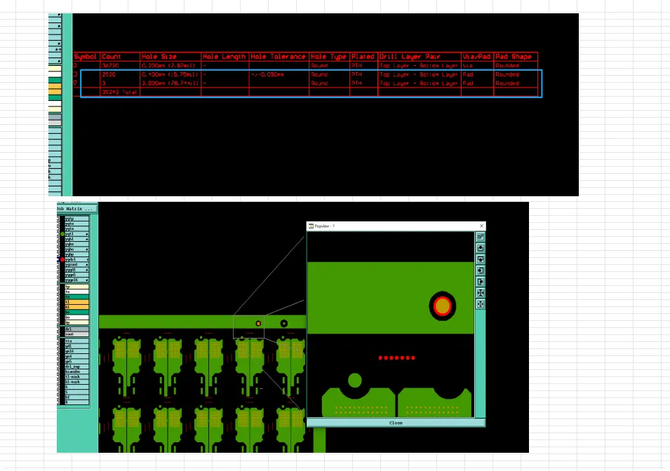
Figure 5: the corresponding pad is smaller than the hole or there is no corresponding pad
Customer Approval of 2 mm Routing Slot Addition
The engineering reply presented the customer with a clear binary choice supported by the evidence table. Option A retained the stamp-hole-only Gerber data and required a written waiver that depanelization force and edge quality remained the customer's responsibility. Option B authorized the factory to insert a standard 2.0 mm routing slot between boards, matching both the order parameter and the PDF, while preserving the existing stamp holes as secondary break-away features. The reply explicitly noted that the 2 mm gap is the minimum practical clearance for the routing bits used on 1.6 mm FR-4 and that zero process edge left no alternative sacrificial material.
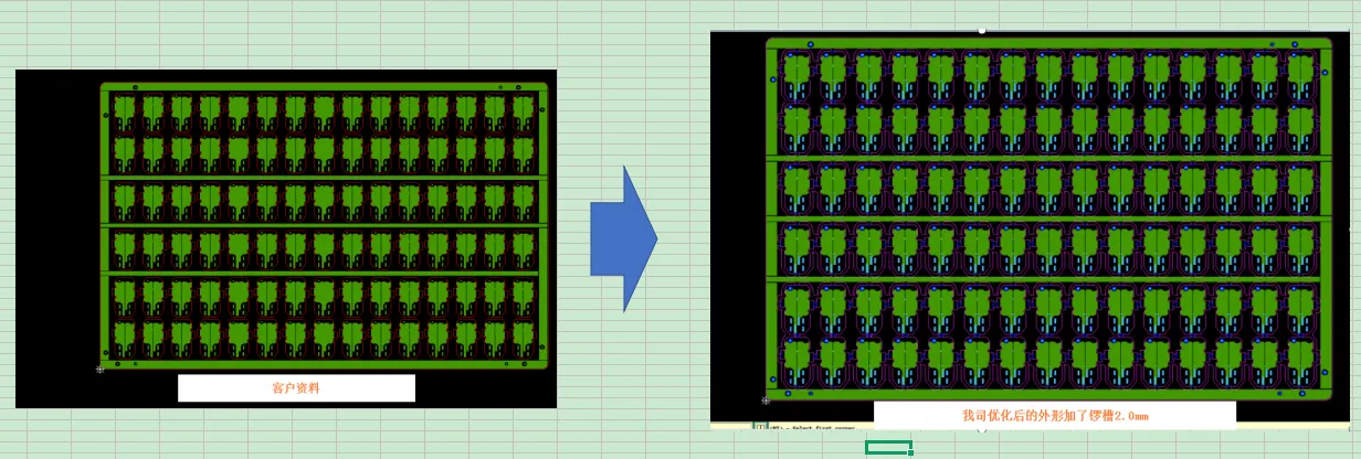
Figure 6: the panelization drawing provided does not include routing gaps
| Engineering Observation | Conflict Identified | Recommended Action | Final Status |
|---|---|---|---|
| Gerber shows stamp holes only; PDF shows routing slots | Documentation inconsistency on separation method | Add 2.0 mm routing slots with customer approval | Approved and implemented |
| Zero process edge, no milling gap in customer panel | Missing clearance for routing bit | Insert factory-standard 2 mm gap | Confirmed |
| PTH attributes without adequate pads | Drill-to-copper definition mismatch | Re-attribute or add pads | Corrected |
| Via openings equal to via diameter | Solder-mask tenting conflict | Close openings to achieve tenting | Updated |
DFM Lessons from Panelization Slot Ambiguity
- When a customer-supplied panel is used, the mechanical layer, panel drawing, and any project PDF must describe the identical separation method; mixed stamp-hole and routing-slot documentation is a primary trigger for Engineering Questions.
- Zero process edge removes all manufacturing margin. Any intended routing slot must already exist in the Gerber data or be explicitly authorized before CAM can add it.
- A 2 mm milling gap is the practical minimum for safe routing-bit clearance on 1.6 mm FR-4; designs that omit this gap force the factory to seek confirmation.
- Stamp holes and continuous routing slots serve different mechanical purposes. Using both is acceptable only when the designer states which feature is primary for dimensional control.
- Hole attributes labeled PTH must be accompanied by pads that satisfy annular-ring rules; otherwise the factory cannot decide whether plating is required.
- Via tenting requirements in fabrication notes must match the actual solder-mask openings in the Gerber files; equal-size openings defeat the tenting intent.
- Board thickness must be identical across all documents; even small discrepancies on a 4-layer stack-up raise stack-up verification holds.
- Provide a single authoritative panelization drawing that includes both the break-away features and the milling gaps so that design intent can be read without cross-document interpretation.
FAQ
Q1: Why does a missing routing gap in a customer panel trigger an Engineering Question?
A1: With zero process edge the factory has no sacrificial material. Adding a routing slot without authorization would alter the board outline. Confirmation is required before any material is removed.
Q2: Can stamp holes and routing slots be used together on the same panel?
A2: Yes, provided the designer states which feature controls the final outline dimensions. Stamp holes then serve only as secondary break-away aids while the routed slots define the edge.
Q3: What is the practical minimum milling gap for a 1.6 mm FR-4 panel?
A3: A 2.0 mm gap is the common factory minimum that allows the routing bit to clear the material without excessive deflection or panel vibration.
Q4: Why do CAM engineers compare Gerber mechanical layers against project PDFs?
A4: The two documents frequently originate from different design stages. When they disagree on routing slots or stamp holes, design intent becomes ambiguous and production cannot proceed safely.
Q5: What happens if PTH holes lack adequate pads?
A5: The annular ring may fall below IPC-6012 limits, or the hole may be non-functional. Either condition requires attribute correction before drilling and plating.
Q6: How does via tenting conflict with equal-size mask openings?
A6: Equal-size openings leave the via barrel exposed. Tenting requires the solder-mask web to cover the via completely; the openings must be closed or reduced to achieve the stated requirement.