










PCB Copper Weight: Why It Controls Performance More Than Layout
What This Video Covers
Many PCBs that appear identical on the surface deliver vastly different thermal and electrical performance because of copper weight—the thickness of the copper foil on each layer, measured in ounces per square foot. This single parameter determines how much current traces can safely carry, how effectively heat is dissipated, and how mechanically robust the board remains under load.
Incorrect copper weight selection often leads to overheating, excessive voltage drop, or unnecessarily high manufacturing costs. The solution is straightforward: base the choice on actual current requirements, power density, and thermal constraints during the design phase.
Engineers working on multilayer PCB, heavy copper PCB, or aluminum PCB projects gain practical guidance for improving reliability while controlling cost. The same principles apply directly to automotive PCB, power supply PCB, and industrial control PCB applications where high current and thermal management are critical.
Key Highlights
- Copper weight sets the actual thickness of every trace and plane, directly governing current-carrying capacity and heat dissipation during PCB fabrication.
- Selecting the correct copper weight prevents overheating, voltage drop, and reliability failures in high-power multilayer and heavy copper designs.
- Proper specification improves performance and cost control for demanding applications such as automotive electronics, power supply units, and industrial control systems.
Understanding Copper Weight and Its Role in PCB Fabrication
Copper weight refers to the standardized thickness of the copper foil laminated onto the core or prepreg layers, expressed in ounces per square foot (oz/ft²). For example, standard 1 oz copper corresponds to approximately 1.37 mils (35 µm) finished thickness after processing, while 2 oz reaches about 2.8 mils. Heavy copper options (3 oz and above) provide significantly greater cross-sectional area.
In manufacturing, copper weight affects etching precision, plating uniformity, and registration accuracy. Higher weights require adjusted etching parameters to avoid undercutting or trace width variations, which can impact impedance control in high-speed designs. During lamination, thicker copper also influences pressure distribution and potential resin flow issues, especially in multilayer boards with many layers.
Proper specification early in the design phase ensures compatibility with the chosen stackup and fabrication process, reducing engineering questions (EQs) and production delays.
How Copper Weight Directly Impacts Current Capacity and Thermal Management
Higher copper weight increases the cross-sectional area of traces and planes, allowing greater current flow with lower I²R losses and reduced temperature rise. According to IPC-2221 standards, a 1 oz trace might safely carry 1–2 A depending on width and temperature rise limits, while 2 oz or heavier copper significantly boosts this capacity.
Thermally, thicker copper acts as a superior heat spreader, lowering junction temperatures in power components and improving overall board reliability under continuous load. In high-power applications, insufficient copper weight often results in hot spots that accelerate material degradation, delamination, or solder joint fatigue.
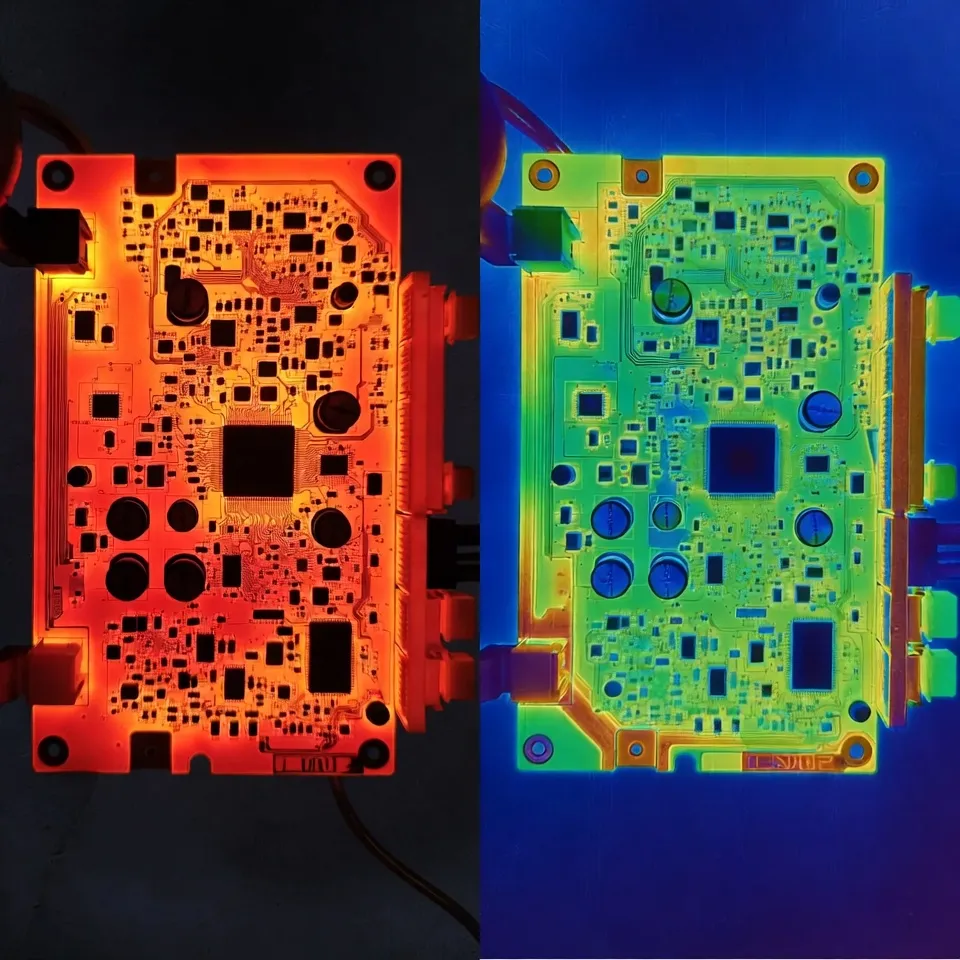
Designers must consider not only external trace width but also internal layers and plane usage when calculating effective thermal paths.
Common Manufacturing Challenges with Incorrect Copper Weight Selection
Selecting too-thin copper for high-current designs frequently causes trace overheating, voltage drop, and eventual field failures such as burned traces or component damage. Conversely, over-specifying heavy copper increases material costs, etching time, and the risk of trace undercut or solder mask adhesion issues due to greater topography.
In production, mismatched copper weights across layers can lead to warpage, registration problems during drilling, or inconsistent impedance. For heavy copper boards, special processes like step etching or differential copper builds may be required, extending lead times if not planned correctly. Real factory cases show that early DFM review of current requirements versus proposed copper weight prevents costly revisions.
Design Optimization Tips for High-Power Applications
Start with accurate current calculations using IPC formulas, factoring in ambient temperature, allowable rise (typically 10–20°C for reliability), and trace length. Prioritize 2 oz or heavier copper on power layers while using 1 oz on signal layers for cost balance in mixed designs.
Incorporate thermal vias under high-power components and consider copper pours or planes for heat spreading. For automotive and industrial applications, validate designs with thermal simulation and prototype testing under worst-case conditions. Collaboration with the fabricator during stackup definition helps optimize copper distribution for both electrical and mechanical performance.
Copper Weight Selection Guide for Different Industries
| Copper Weight | Typical Thickness (mils) | Current Capacity Example (10°C rise, 10mm trace) | Best Applications | Key Considerations |
|---|---|---|---|---|
| 1 oz | 1.37 | ~1.5–2 A | Consumer, low-power signal | Cost-effective, standard process |
| 2 oz | 2.8 | ~3–4 A | Power supply, industrial control | Good balance of performance and cost |
| 3 oz+ (Heavy) | 4.2+ | 5 A and above | Automotive, high-power, new energy | Enhanced thermal/mechanical strength, higher cost |
This table serves as a practical reference; always verify with specific design tools and manufacturer capabilities.
FAQ
Q1: How does copper weight affect current capacity and thermal performance in a PCB?
A1: Copper weight directly determines the thickness of every trace and copper plane. Higher copper weight increases the cross-sectional area, allowing traces to carry significantly more current without excessive heating while improving overall thermal dissipation across the board.
Q2: What are the manufacturing cost and reliability trade-offs of using thicker copper weights?
A2: Thicker copper raises material and etching costs during PCB fabrication, but it greatly improves mechanical strength, heat spreading, and long-term reliability. Thinner copper lowers production cost yet limits current handling and increases the risk of overheating or voltage drop in high-power designs.
Q3: When should designers specify heavy copper PCB instead of standard copper for high-power applications?
A3: Heavy copper PCB (typically 3 oz and above) should be chosen when the design requires high current capacity, superior thermal management, or greater mechanical robustness-common in automotive electronics, power supply units, industrial control systems, and new-energy applications.
Q4: How does copper weight influence PCB etching and impedance control during fabrication?
A4: Thicker copper requires longer etch times and tighter process control to maintain trace width tolerances. This can affect impedance consistency, especially in RF or high-speed designs. Fabricators often recommend compensation adjustments in the Gerber files and may suggest symmetric stackups to minimize warpage risks.
Q5: Can different copper weights be used on the same multilayer PCB?
A5: Yes, asymmetric copper builds (e.g., 2 oz on outer power layers and 1 oz on inner signal layers) are common to optimize cost and performance. However, this requires careful DFM review to ensure balanced lamination, registration, and thermal expansion compatibility.
Why can two PCBs look identical but behave very differently with heat and current?
Many people assume the difference comes from components or layout.
In reality, the key factor is copper weight.
Copper weight is the thickness of copper on a PCB layer, usually measured in ounces per square foot.
It sets the base thickness of all traces, determining how much current they can carry.
Thicker copper improves heat dissipation, mechanical strength, and reliability under high power.
Choosing the wrong copper weight can cause overheating, voltage drop, or higher manufacturing cost.
When designing a PCB, select copper weight based on current requirements, power levels, and thermal needs.
This is aivon, making PCB learning easier, comment below — and follow for more PCB tips!





