










PCB Back Drilling: Precision Removal of Via Stubs in High-Speed Designs
What This Video Covers
In high-speed PCB designs, unused portions of plated vias create "stubs" that cause signal reflections, impedance discontinuities, and performance degradation. This video provides a clear explanation of PCB back drilling — a precision secondary drilling technique used to remove these non-functional via sections after plating.
The content details the process: a larger drill removes the unused plated barrel from the opposite side of the board. It highlights major challenges including precise depth control (too shallow leaves a stub; too deep damages active layers), drill misalignment risks, and dependencies on board thickness, via aspect ratio, and manufacturer capabilities.
Viewers learn best practices for specifying start layers, stop depths, and maximum residual stub length in fabrication documentation. Back drilling is a valuable tool for high-frequency PCB, HDI PCB, and complex multilayer boards where signal integrity is critical.
This technique helps achieve reliable performance in demanding applications such as aerospace PCB, automotive electronics, and telecommunication systems, though it should be applied selectively due to added cost.
Key Highlights
- Via Stub Issue: Unused via sections act as stubs that reflect signals and degrade high-speed performance.
- Back Drilling Process: Secondary drilling from the opposite side removes non-functional plated barrel while preserving active signal paths.
- Critical Controls: Precise depth specification, alignment, and manufacturer capabilities determine success and residual stub length.
Understanding Via Stubs and Their Impact on Signal Integrity
Unused via sections in multilayer PCBs function as resonant stubs that create impedance mismatches and signal reflections, particularly problematic above 5 Gbps. These stubs act as open transmission line segments, leading to increased insertion loss, jitter, and potential bit errors in high-speed digital interfaces.
In production environments, via stubs become more significant as layer counts increase and signal rise times decrease. The electrical length of the stub relative to the signal wavelength determines the severity of reflections. For designs operating in the GHz range, even short stubs of 20-30 mils can degrade performance noticeably.
Manufacturers observe that uncontrolled stubs contribute to field failures in high-reliability applications. Proper via design combined with back drilling minimizes these issues by effectively shortening the stub to an acceptable residual length, typically targeting less than 10-15 mils depending on frequency requirements.
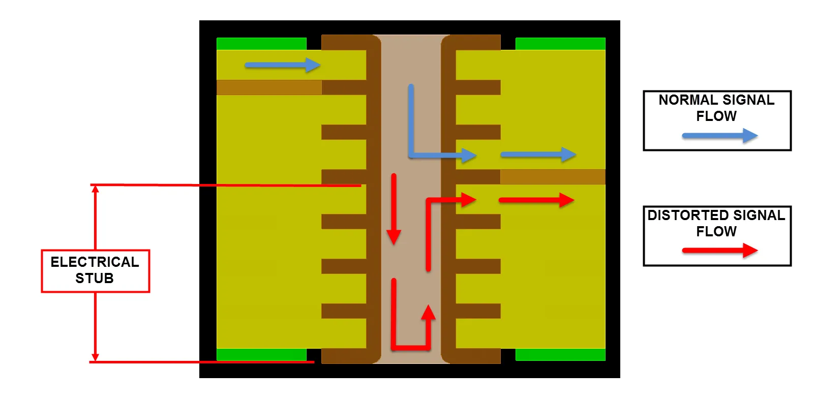
The PCB Back Drilling Process: Step-by-Step Manufacturing Overview
PCB back drilling begins after initial via plating and before solder mask application. Using CNC-controlled equipment, a larger diameter drill bit approaches from the secondary side of the board to remove the non-functional plated copper barrel. Depth is tightly controlled through precise Z-axis programming and depth-sensing technology.
Key process parameters include drill diameter (typically 8-12 mils larger than the via), spindle speed, feed rate, and vacuum settings to manage debris evacuation. The operation requires excellent registration accuracy between the primary drill and back drill programs to prevent offset damage to functional traces or pads.
Post-drilling inspection verifies residual stub length through cross-section analysis or time-domain reflectometry (TDR) measurements. Production teams must balance cycle time increases against signal performance gains, making this a selective process rather than a standard operation.
Critical DFM Considerations for Effective Back Drilling
| Parameter | Typical Range | Impact on Process | Recommendation |
|---|---|---|---|
| Board Thickness | 62-120 mils | Affects drill depth tolerance | Specify clearly in fab notes |
| Via Aspect Ratio | 8:1 to 12:1 | Influences plating uniformity | Keep below 10:1 when possible |
| Residual Stub Length | 5-15 mils | Determines signal performance | Define maximum allowable per net |
| Back Drill Diameter | Via + 8-12 mils | Ensures complete stub removal | Coordinate with fabricator |
Designers should include back drilling callouts in fabrication drawings with clear start/stop layers and maximum stub tolerances. Collaboration with the manufacturer during the DFM review stage helps identify potential issues related to panel thickness variation and material movement. Accurate stackup documentation and layer numbering prevent costly errors in depth programming.
Manufacturing Challenges and Risk Mitigation Strategies
Depth control remains the primary challenge in PCB back drilling. Variations in board thickness, material compression, and drill wear can result in inconsistent stub removal. Too shallow drilling leaves residual stubs, while excessive depth risks damaging inner layer connections or causing delamination.
Drill misalignment represents another significant risk, potentially creating elliptical holes or damaging adjacent features. Advanced fabricators employ laser depth control and optical registration systems to improve accuracy, but these capabilities vary across manufacturers.
Practical recommendations include providing multiple depth targets when possible and conducting first-article verification with cross-sectioning. For high-volume production, statistical process control on back drill depths helps maintain consistency. Designers should also consider alternative techniques such as blind vias or optimized via placement when back drilling costs become prohibitive.
When to Specify Back Drilling in High-Frequency PCB Projects
Back drilling provides the greatest return on investment for signals exceeding 5-10 Gbps or in applications with stringent eye diagram requirements. It is commonly applied to clock signals, high-speed serial links, and RF traces in aerospace, automotive radar, and 5G infrastructure boards.
Cost-benefit analysis should consider the added manufacturing steps, increased scrap risk, and testing requirements. For lower-speed designs or short vias, other DFM strategies such as reducing layer count or using buried vias may offer better overall value.
Fabrication documentation must clearly identify which vias require back drilling to avoid unnecessary processing. Close communication with the chosen manufacturer ensures the process aligns with their equipment capabilities and quality standards.
FAQ
Q1: What problem does back drilling solve in PCBs?
A1: Back drilling removes unused via stubs that cause signal reflections, impedance mismatches, and integrity issues in high-speed designs.
Q2: What are the main challenges with back drilling?
A2: Depth control is critical — too shallow leaves a stub, too deep damages functional layers. Drill tolerance and misalignment also affect results.
Q3: When is back drilling worth the extra cost?
A3: Apply back drilling selectively for high-speed signals (typically >5–10 Gbps) where stub length significantly impacts performance and signal integrity.
Q4: How does back drilling differ from using blind or buried vias?
A4: Back drilling is a post-plating mechanical process applied to through vias, while blind and buried vias are formed during the initial lamination and drilling sequence. Back drilling is often more cost-effective for selective high-speed nets in thick boards, whereas blind vias require additional lamination cycles and tighter process controls.
Q5: What documentation is needed to specify back drilling properly?
A5: Provide clear layer start/stop information, maximum residual stub length per net or net class, and preferred drill diameter offsets. Include notes on tolerance requirements and reference any relevant IPC standards for via quality verification.
Your signal doesn't use the whole via — so what happens to the rest?
The unused section forms a stub.
And it can interfere with your signal more than you expect.
That's where back drilling comes in.
Back drilling is a secondary drilling process after plating.
A larger drill enters from the opposite side.
It removes the unused plated section of the via barrel.
Depth control is the main challenge.
Too shallow leaves an electrically significant stub.
Too deep can cut into the active signal layer.
Drill misalignment can also reduce effectiveness.
Results depend on board thickness, via aspect ratio, and drill tolerance.
Fabrication capability varies between manufacturers.
Define start layer and stop depth clearly in your drill table.
Check the required residual stub length.
And only apply back drilling when signal performance justifies the added cost.





