 00:58
00:58
PCB Via Stubs
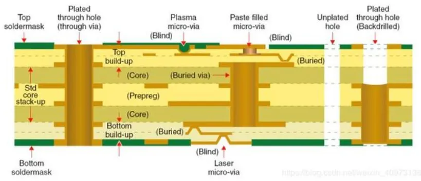
PCB via stubs represent a critical consideration in modern printed circuit board (PCB) design, particularly for high-speed and high-frequency applications. These stubs occur when a via extends beyond the signal layer it connects, creating an unused portion that acts as a resonant stub. This can lead to signal integrity issues such as reflections, impedance discontinuities, and increased insertion loss, which degrade performance in circuits handling gigabit data rates or RF signals. Engineers searching for information on PCB via stubs often seek ways to mitigate these effects to ensure reliable board functionality, especially in industries like telecommunications, aerospace, and consumer electronics where signal quality is paramount. Understanding the impact of via stubs begins with recognizing their formation in multilayer PCBs. During the design phase, vias that traverse multiple layers without termination can introduce parasitic capacitance and inductance, potentially causing signal distortion or electromagnetic interference. Best practices include minimizing stub length through techniques like backdrilling, where excess via material is removed from the backside of the board, or employing blind and buried vias to avoid stubs altogether. These methods not only enhance signal integrity but also reduce manufacturing costs by optimizing layer stackups and routing strategies. For instance, in differential pair routing, careful via placement can prevent mode conversion and crosstalk, leading to more robust designs. The articles gathered under the PCB Via Stubs tag delve into these topics with practical examples, simulation tools, and case studies. Readers can find guidance on selecting appropriate via types for specific applications, calculating stub resonance frequencies, and integrating stub mitigation into CAD workflows. Whether you are troubleshooting existing designs or planning new ones, these resources offer actionable insights to improve PCB performance and reliability, helping you address common challenges in high-speed electronics development.
Video Guide
-
00:58
Technical Articles