Volatile memory is the high-speed workspace that enables processors to execute code and manipulate data in real time. In PCB design and fabrication, the selection of DRAM versus SRAM, the specific DDR generation, and the speed grade directly determine trace routing rules, impedance targets, stack-up symmetry, via technology, power delivery network (PDN) design, and long-term board reliability. Aivon's expertise in advanced PCB manufacturing ensures these memory interfaces achieve optimal signal integrity, manufacturability, and performance across automotive, industrial, networking, and consumer electronics applications.
DRAM Cell Architecture and Data Storage Principles
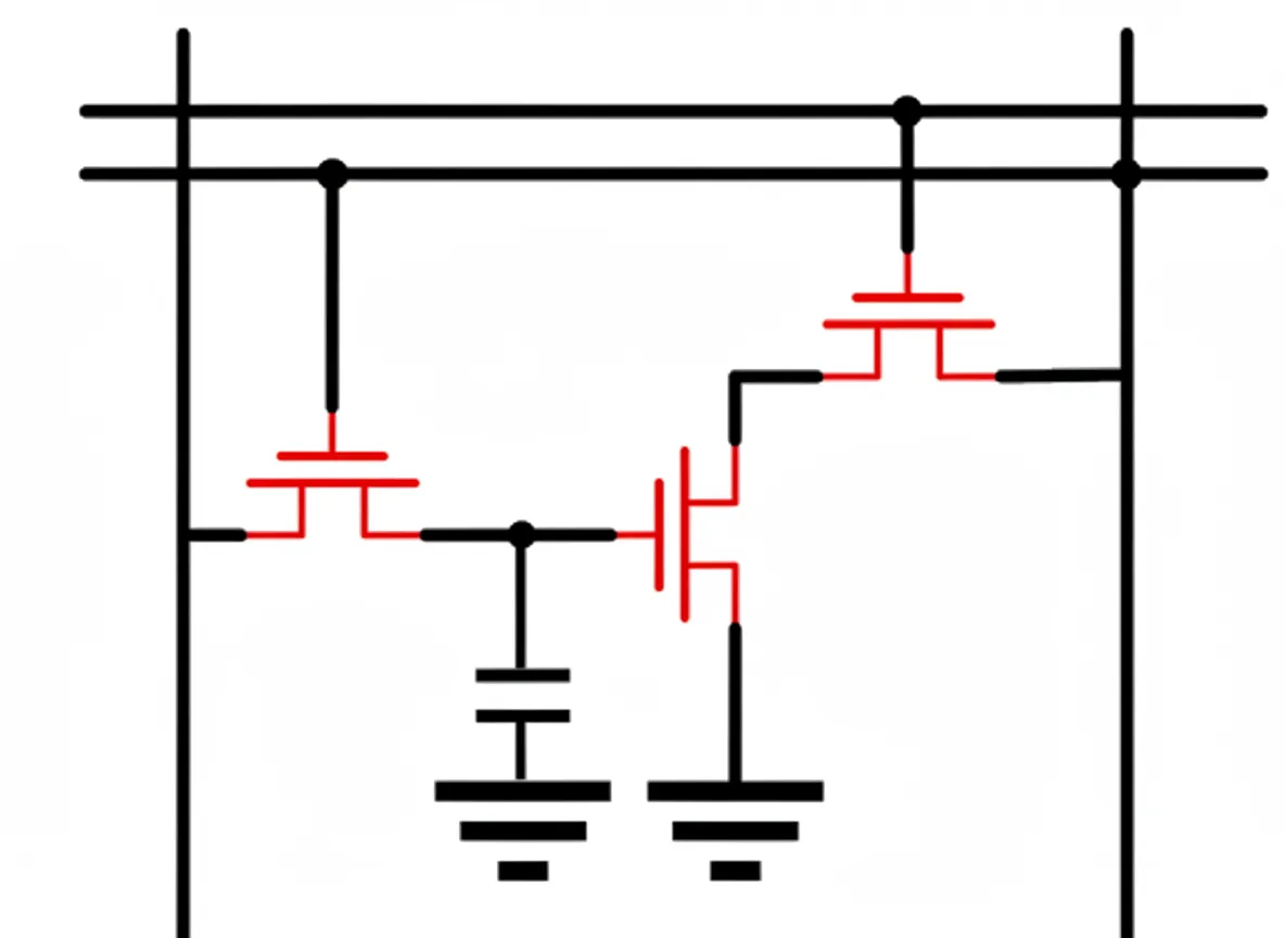
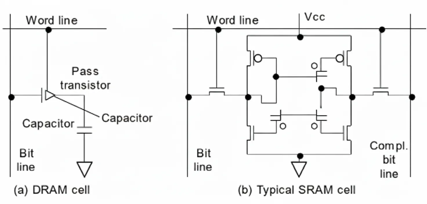
DRAM stores each bit as charge in a capacitor controlled by a single access transistor. When the word line is asserted, the transistor connects the storage capacitor to the bit line, allowing the sense amplifier to detect a small voltage differential and determine the stored logic level. Because capacitors leak charge, every row must be refreshed periodically—typically every 64 ms in standard DRAM.
On the PCB, this architecture translates into a high-pin-count interface with multiplexed address/command lines and bidirectional data strobes (DQS). Engineers must implement precise length matching (often within ±5–10 mil), controlled impedance (40–60 Ω single-ended, 80–120 Ω differential), and robust termination schemes. The periodic refresh commands add bus traffic that affects overall timing budgets and requires careful placement of the memory controller relative to the DRAM devices.
How DRAM Stores, Reads, and Refreshes Data
A read operation begins with precharge of the bit lines, followed by word-line activation and sensing. Write operations drive the bit lines to the desired voltage before activating the word line. Refresh is performed by reading a row and immediately writing the data back, restoring capacitor charge.
From a PCB perspective, these operations demand clean power rails and minimal noise on address/command buses. Refresh timing must be respected in firmware and memory controller settings; failure to do so results in data corruption that manifests as intermittent bit errors during system validation. Proper decoupling capacitor placement and power plane design are essential to support the current spikes during row activation.
SRAM Basic Circuits and Operating Principles
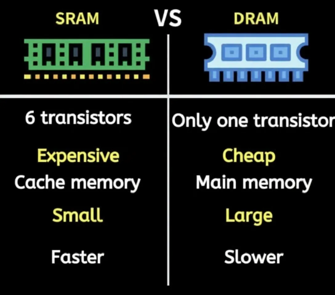
SRAM uses a six-transistor (6T) flip-flop cell consisting of two cross-coupled inverters and two access transistors. The bistable latch holds data indefinitely as long as power is supplied, eliminating the need for refresh. Access is faster and deterministic because no sense-amplifier settling or refresh overhead exists.
PCB implications are favorable: simpler timing relaxes length-matching tolerances, reduces the need for on-die termination (ODT), and allows shorter traces. SRAM's larger cell size limits density, so it is typically used for cache, FIFOs, or configuration memory where low latency outweighs capacity requirements. Its lower pin count and often smaller packages simplify routing and reduce layer count in dense layouts.
DRAM vs SRAM: PCB Design Trade-offs
- Density and Cost — DRAM offers far higher bit density at lower cost per bit; SRAM remains practical only for small, speed-critical blocks.
- Speed and Latency — SRAM provides single-cycle access with minimal controller complexity; DRAM requires multiple clock cycles and careful timing closure.
- Power Consumption — Both lose all data when power is removed. DRAM adds continuous refresh current; self-refresh modes in modern DRAM reduce but do not eliminate this overhead. PCB power sequencing and voltage rail design must accommodate these differing profiles.
- Board Real Estate and Routing — SRAM simplifies layout; DRAM demands extensive length matching, impedance control, and often more layers or HDI features.
DDR3 versus DDR4: Technical Evolution and PCB Impact
DDR4 doubles the maximum data rate of DDR3 while lowering core voltage from 1.5 V / 1.35 V to 1.2 V. It introduces bank grouping, improved burst lengths, and more sophisticated on-die termination that reduces power and improves signal integrity at higher speeds.
PCB-level differences include:
- DDR4 supports data rates up to 3200 MT/s and beyond, requiring tighter impedance control and often back-drilled vias.
- Lower voltage reduces heat but demands cleaner PDN with additional decoupling capacitors placed near DRAM balls.
- Finer ball pitch in DDR4 packages influences via drill size, pad design, and stack-up symmetry.
Bandwidth calculations illustrate the gains: a DDR3-1600 module (1600 MT/s × 64 bits / 8 = 12.8 GB/s per channel) is surpassed by DDR4-3200 at 25.6 GB/s. These numbers assume ideal conditions; real-world performance depends on controller efficiency and PCB signal integrity.
DDR4-3200 versus DDR4-3600: Speed Grades and Layout Constraints
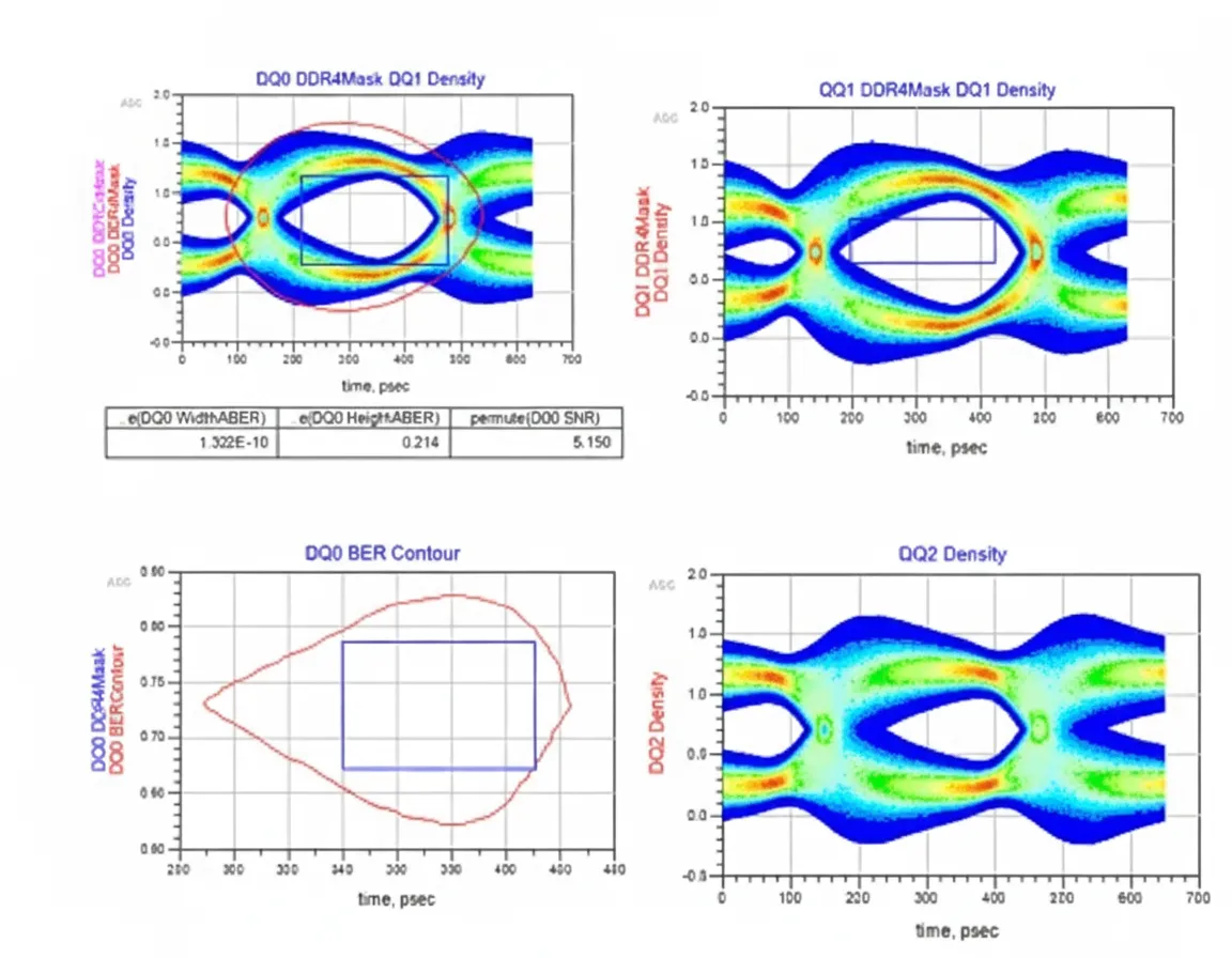
The 3600 MT/s grade delivers roughly 12.5 % higher theoretical bandwidth than 3200 MT/s. Higher speeds shrink timing margins and impose stricter PCB rules: shorter maximum trace lengths, tighter intra-pair and inter-pair skew, and more precise differential impedance targets. Via stub effects become more pronounced, often necessitating back-drilling or blind/buried via structures. Cost increases for both the DRAM devices and the tighter fabrication tolerances required.
Via Stub Effects on DDR4 Parallel Links
Long via stubs create impedance discontinuities that generate reflections and ringing, degrading eye opening at multi-gigabit speeds. PCB manufacturing solutions include controlled-depth back-drilling to remove unused via barrel segments, or blind/buried vias that avoid stubs entirely. Early collaboration with the fabricator on stack-up and via technology is critical to maintain signal integrity margins.
Power Behavior, Data Retention, and PCB Power Design
Both DRAM and SRAM are volatile—data disappears without power. DRAM additionally requires refresh even in standby. Modern DRAM supports self-refresh modes that lower power, yet PCB designers must still provide stable, low-noise voltage rails and proper power sequencing to prevent corruption during power-up or power-down events. Decoupling strategies and plane capacitance become especially important for high-density memory arrays.
Manufacturing, Reliability, and Design-for-Manufacturability
High-speed memory PCBs require low-loss laminates, precise impedance control through etching and dielectric thickness tolerances, and robust copper balance to prevent warpage. Thermal vias under DRAM packages and appropriate copper weight help manage heat. Common failure mechanisms include bit errors from marginal signal integrity, electromigration in power vias, and mechanical stress from CTE mismatch. Rigorous DFM reviews, electrical testing, and impedance verification at the fabrication stage maximize yield and long-term reliability.
Future Trends in Memory Technology and PCB Implications
The memory landscape continues to evolve rapidly, driven by AI, 5G/6G, edge computing, and data-center demands. DDR5 is entering mainstream adoption with data rates starting at 4800 MT/s and scaling beyond 6400 MT/s, featuring on-die ECC, improved power efficiency at 1.1 V, and decision-feedback equalization (DFE) that further tightens PCB signal-integrity requirements. Designers must adopt lower-loss laminates, finer feature sizes, and advanced via structures such as stacked microvias or hybrid HDI to support these speeds.
High Bandwidth Memory (HBM) and HBM3/HBM3E stack DRAM dies vertically on a silicon interposer, delivering terabyte-per-second bandwidth but requiring 2.5D/3D packaging expertise and specialized PCB substrates with ultra-fine lines and spaces. LPDDR5X and upcoming LPDDR6 target mobile and automotive applications with even lower power and higher densities, influencing flexible or rigid-flex PCB stack-ups and thermal management strategies.
Compute Express Link (CXL) enables memory expansion and disaggregation, shifting some high-speed signaling from parallel DDR buses to serial PCIe-based links that demand different routing topologies and impedance profiles. Emerging non-volatile memories such as MRAM and ReRAM are being explored for hybrid volatile/non-volatile architectures, potentially reducing refresh overhead while introducing new layout and reliability considerations.
Sustainability pressures are pushing lower-power memory solutions and halogen-free, high-Tg materials. PCB manufacturers must therefore invest in advanced materials, tighter process controls, and simulation-driven design to keep pace with these trends.
Conclusion
By integrating memory architecture decisions into every stage of PCB design—from schematic and stack-up through layout and fabrication—engineers achieve the optimal balance of performance, cost, and reliability. As memory interfaces continue to push speed and density boundaries, close collaboration between system designers and PCB fabricators becomes essential. Aivon delivers the precision impedance control, advanced via technologies, low-loss material expertise, and high-reliability assembly needed to realize these demanding memory interfaces from prototype to volume production, helping customers stay ahead in an increasingly complex electronics landscape.