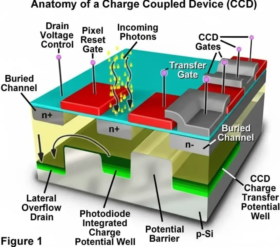
CMOS Image Sensors (CIS) have become the dominant technology for digital imaging in smartphones, automotive cameras, industrial vision systems, and medical devices. Unlike older CCD sensors, CIS integrate photodetection, amplification, and readout circuitry on the same silicon chip, offering advantages in power consumption, speed, and system-on-chip integration.
Fundamentals of Image Quality and Pixel Performance
Image quality is largely determined by pixel-level characteristics. Key metrics include full-well capacity (maximum charge storage), quantum efficiency (photon-to-electron conversion), sensitivity, dark current, and crosstalk. Signal-to-noise ratio (SNR) is a primary indicator of performance, particularly challenging in low-light conditions where multiple noise sources must be minimized.
Evolution of Pixel Technology
Pixel sizes have shrunk dramatically to support higher resolutions. Early improvements focused on microlenses and back-side illumination (BSI) to boost light collection. Subsequent generations addressed optical and electrical crosstalk using deep trench isolation and advanced gate structures. Modern sub-micron pixels often employ Quad (or Tetra) architectures, grouping multiple photodiodes under shared color filters and readout circuitry to enhance low-light performance.
CMOS Image Sensor Structure and Operation
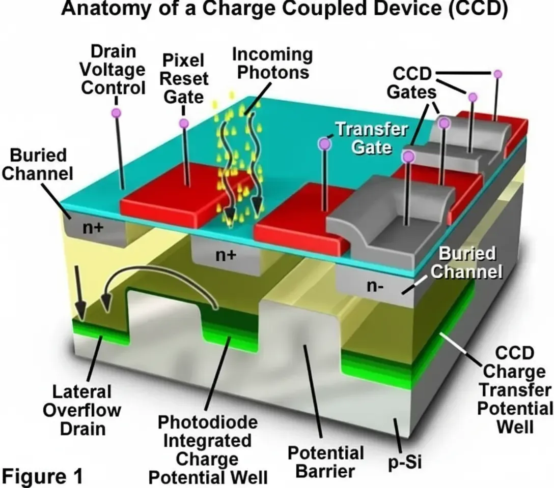
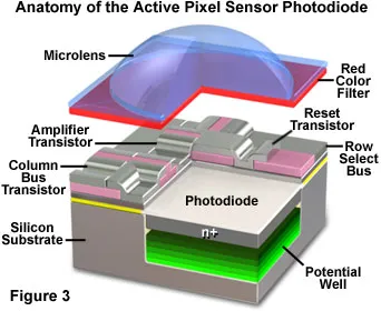
CIS pixels typically consist of a photodiode, transfer gate, floating diffusion, and in-pixel amplifiers (source follower, reset, and select transistors). Light generates electron-hole pairs in the silicon photodiode; collected charge is converted to voltage and read out row by row.
Color imaging relies on Bayer mosaic filters (RGGB pattern) placed over the pixel array, with microlenses concentrating light onto the active photodiode area. Fill factor - the proportion of photosensitive area per pixel - directly impacts sensitivity; microlenses and BSI help maximize it.
Key Technical Challenges and Solutions
- Noise Management: Sources include photon shot noise, dark current, reset (kTC) noise, and thermal noise. Techniques such as correlated double sampling (CDS) and fixed-pattern noise (FPN) correction significantly improve image quality.
- Dynamic Range and Speed: High dynamic range (HDR) modes and fast readout support applications requiring both bright and dark scene capture or high frame rates.
- Quantum Efficiency: Wavelength-dependent losses (especially blue and near-IR) are mitigated through process optimizations and material choices.
Fabrication and Process Considerations
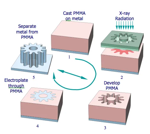
CIS fabrication leverages CMOS-compatible processes, enabling integration with logic circuitry. Back-side illumination separates the optical path from wiring layers, improving performance. Stacked sensor designs (pixel array + logic die) further enhance functionality and yield.
PCB Design and Manufacturing for Camera Modules
Reliable camera module performance depends on the supporting printed circuit board:
- High-Speed Interfaces: MIPI CSI-2 or other high-speed serial links require controlled impedance routing, length matching, and noise isolation.
- Power Integrity: Clean, low-noise supplies for analog sections; multiple power domains and decoupling are essential.
- Thermal Management: Heat from high-resolution sensors and processors must be dissipated without introducing thermal noise or mechanical stress.
- Mechanical Precision: Accurate alignment for lens assemblies and robust SMT processes for miniature components.
Rigid-flex PCBs are common in compact modules to accommodate folding or space constraints while maintaining signal integrity. Advanced assembly techniques ensure high yield for fine-pitch connectors and optical components.
Applications and Industry Trends
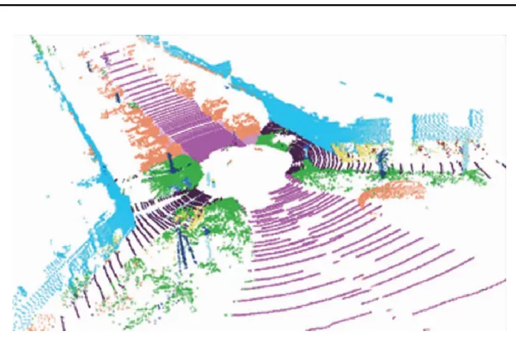
CIS technology powers smartphones, automotive surround-view and ADAS cameras, machine vision, and medical endoscopy. Trends include higher resolutions, better low-light performance, 3D sensing (structured light or ToF), and AI-enhanced on-chip processing.
Continued innovation in pixel architectures, stacking, and materials drives performance while demanding sophisticated PCB fabrication and assembly capabilities to realize full system potential.
Optional FAQ Section
Q1: What is the difference between CCD and CMOS image sensors?
A1: CMOS sensors integrate amplification and readout per pixel or column, offering lower power and higher integration; CCDs transfer charge across the array, traditionally excelling in certain noise characteristics but now largely superseded in consumer applications.
Q2: Why is PCB design important for camera modules?
A2: It ensures signal integrity for high-speed data, stable power delivery, thermal dissipation, and mechanical reliability critical to overall image quality and module performance.
Q3: What are Quad pixels in modern CIS?
A3: An architecture where four photodiodes share readout circuitry and color filters to improve sensitivity and reduce noise in small-pixel, high-resolution sensors.