MEMS (Micro Electro Mechanical Systems) integrate mechanical structures, sensors, actuators, and electronic circuitry on a single substrate through microfabrication. These devices convert physical inputs into electrical signals or mechanical motion and are foundational to many sensor and actuator applications in automotive, industrial, and consumer electronics.
MEMS processing adapts conventional semiconductor techniques such as thin-film deposition, photolithography, and etching, while introducing specialized steps to create three-dimensional mechanical features.
Wafer Technologies in MEMS
Silicon-on-Insulator (SOI) wafers consist of a single-crystal silicon device layer separated from the handle wafer by a buried oxide layer. In MEMS fabrication the oxide serves as an effective etch stop during silicon removal, enabling precise control of membrane thickness and the creation of suspended structures such as cantilevers or diaphragms.
TAIKO grinding preserves the outer wafer edge while thinning only the central region. This approach reduces wafer warpage, increases mechanical strength, and improves handling of thinned substrates compared with conventional full-surface grinding. Supporting wafers combined with thermal-release films further facilitate processing of ultra-thin wafers by providing temporary mechanical stability during subsequent steps.
Wafer Bonding Techniques
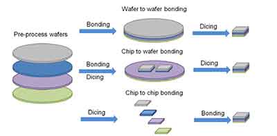
Wafer bonding joins two substrates either directly or through an intermediate layer. Direct bonding relies on intermolecular forces activated by thermal annealing and is commonly used to fabricate SOI wafers. Intermediate-layer bonding employs adhesives, polymers, or metals to accommodate surface topography or dissimilar materials. Both methods must control bond strength, hermeticity, and residual stress to prevent delamination or warping in finished MEMS devices.
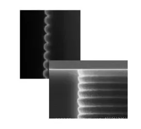
Etching Processes
Reactive ion etching (RIE) generates plasma containing ions and neutral radicals. Ions enable directional (anisotropic) etching, while radicals produce isotropic material removal. The Bosch process alternates cycles of silicon etching with polymer deposition and polymer removal from horizontal surfaces. This sequence achieves high-aspect-ratio trenches with vertical sidewalls, although the cyclic nature produces a characteristic scalloped sidewall profile that can influence mechanical stress distribution and fluidic behavior in MEMS structures.
Atomic Layer Deposition (ALD)
ALD builds films one atomic layer at a time through sequential precursor exposure and purge steps that rely on self-limiting surface reactions. The technique delivers exceptional thickness uniformity and conformality, even on high-aspect-ratio features, narrow gaps, and deep vias. In MEMS, ALD is applied for protective coatings, dielectric layers, and polymer deposition steps within deep-etch sequences.
Design and Manufacturing Considerations
MEMS fabrication imposes strict requirements on material properties, process control, and dimensional tolerances. SOI layer thickness uniformity, oxide quality, and handle-wafer flatness directly affect device performance. TAIKO grinding and temporary bonding must maintain alignment accuracy while minimizing stress that could fracture delicate mechanical elements. Etch selectivity, polymer residue removal, and scallop amplitude control are critical for achieving target mechanical resonance frequencies and long-term reliability. ALD film stress, step coverage, and precursor compatibility influence electrical isolation and environmental stability.
These processes are typically qualified through thermal cycling, mechanical shock, humidity exposure, and accelerated life testing to verify performance under end-use conditions.
Applications in Sensors and Actuators
MEMS devices fabricated with these technologies appear in pressure sensors, accelerometers, gyroscopes, microphones, and microfluidic components. Automotive safety systems, industrial process control, and consumer electronics all rely on the precision and miniaturization enabled by SOI-based structures, deep silicon etching, and conformal ALD coatings.
Industry Trends and System Integration
Continued miniaturization and multi-sensor integration drive demand for tighter process control and hybrid substrates. Integration of MEMS with CMOS electronics on the same die or within the same package increases the importance of compatible thermal budgets, stress management, and interconnect technologies. These trends reinforce the need for robust design-for-manufacturability practices across wafer-level processing.
PCB and Electronic Manufacturing Relevance
Many MEMS process steps parallel techniques used in HDI PCB and flexible circuit fabrication. Photolithography and etching define fine features on both silicon and copper-clad laminates. ALD and other thin-film deposition methods share principles with surface finishes and dielectric coatings applied to PCBs. Wafer bonding and temporary carrier techniques resemble lamination and carrier-supported processing of thin flexible substrates. SOI and thinned-wafer handling considerations inform material selection and stress management when producing thin-core or metal-core PCBs for sensor modules.
Reliability engineering practices developed for MEMS—such as control of residual stress, hermetic sealing, and environmental qualification—translate directly to automotive-grade and industrial PCB assemblies that must survive vibration, thermal shock, and contamination. High-density interconnect (HDI) and flexible printed circuit (FPC) technologies enable compact integration of MEMS sensors with signal-conditioning electronics, supporting the same miniaturization and performance goals pursued in MEMS fabrication.
Conclusion
MEMS fabrication relies on specialized wafer preparation, bonding, deep etching, and atomic-layer deposition to create functional three-dimensional structures. Each process introduces specific material, dimensional, and reliability constraints that must be addressed through precise process control and qualification. These same microfabrication principles and manufacturing disciplines underpin the production of advanced PCBs, flexible circuits, and integrated sensor modules, enabling reliable electronic systems that incorporate MEMS devices.