 00:58
00:58
PCB Back Drilling
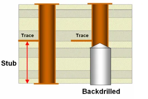
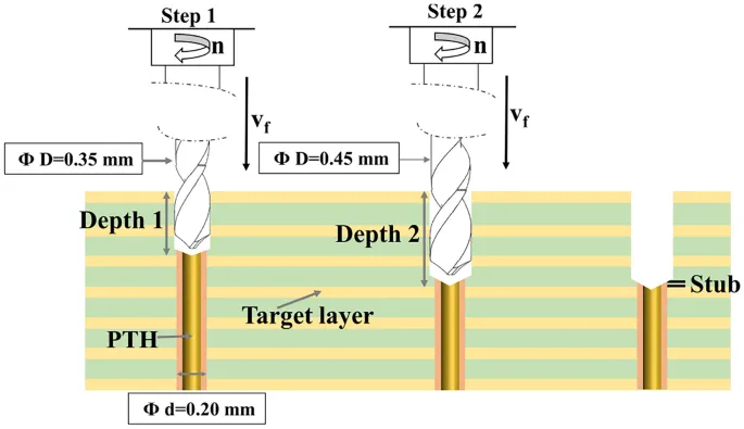
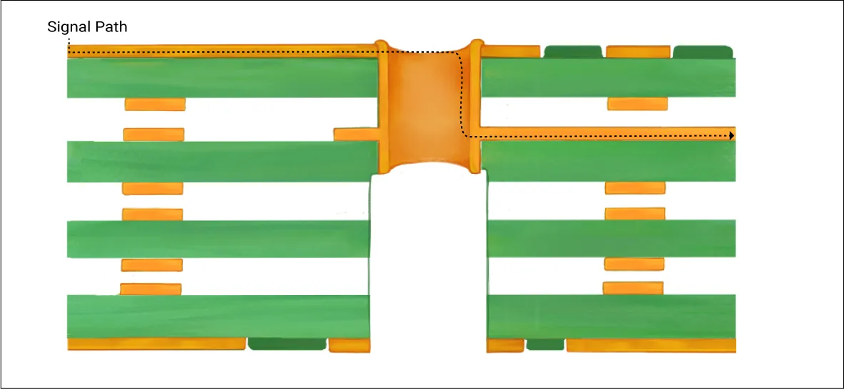
PCB back drilling is a specialized manufacturing technique used in printed circuit board (PCB) design to enhance signal integrity in high-speed and high-frequency applications. This process involves removing the unused portion of plated through-hole vias, known as stubs, by drilling from the opposite side of the board after initial fabrication. By eliminating these stubs, which can cause signal reflections and distortions, back drilling ensures cleaner transmission paths, reduces electromagnetic interference, and maintains consistent impedance across layers. Engineers and designers searching for information on PCB back drilling often seek solutions to optimize performance in multilayer boards, where via stubs pose significant challenges in modern electronics. The practical applications of PCB back drilling extend to industries such as telecommunications, data centers, aerospace, and automotive electronics, where reliable high-speed data transfer is critical. For instance, in designs operating at frequencies above 10 GHz, back drilling can significantly lower bit error rates and improve overall system efficiency. Best practices include careful via depth calculation during the design phase to determine the exact drilling depth, selecting appropriate drill bits to avoid damaging inner layers, and conducting thorough post-drilling inspections to verify stub removal without compromising board integrity. Designers should also consider factors like board thickness, layer count, and material properties to decide if back drilling is necessary, balancing cost with performance gains. This tag on PCB back drilling gathers a collection of articles that delve into these techniques, offering detailed guides on implementation, case studies from real-world projects, and comparisons with alternative methods like blind vias. Readers can find valuable insights into troubleshooting common issues and integrating back drilling into their PCB workflows for superior results.
Video Guide
-
00:58
Technical Articles
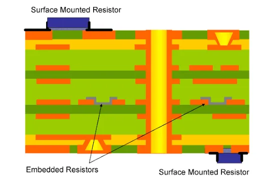
20-Layer Embedded-Resistor PCB: Process Flow and Core Manufacturing Challenges
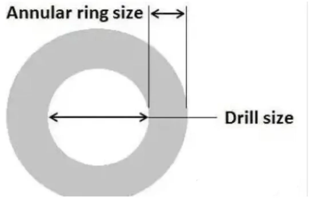
Padless Holes on a PCB: Why Designers Remove the Annular Ring

Why Backdrill Stubs Can Still Be Too Long After the Layer Pair Is Correct
How to Resolve Backdrill, Press-Fit & Copper Balance Issues in 3mm 24-Layer FR4 PCB
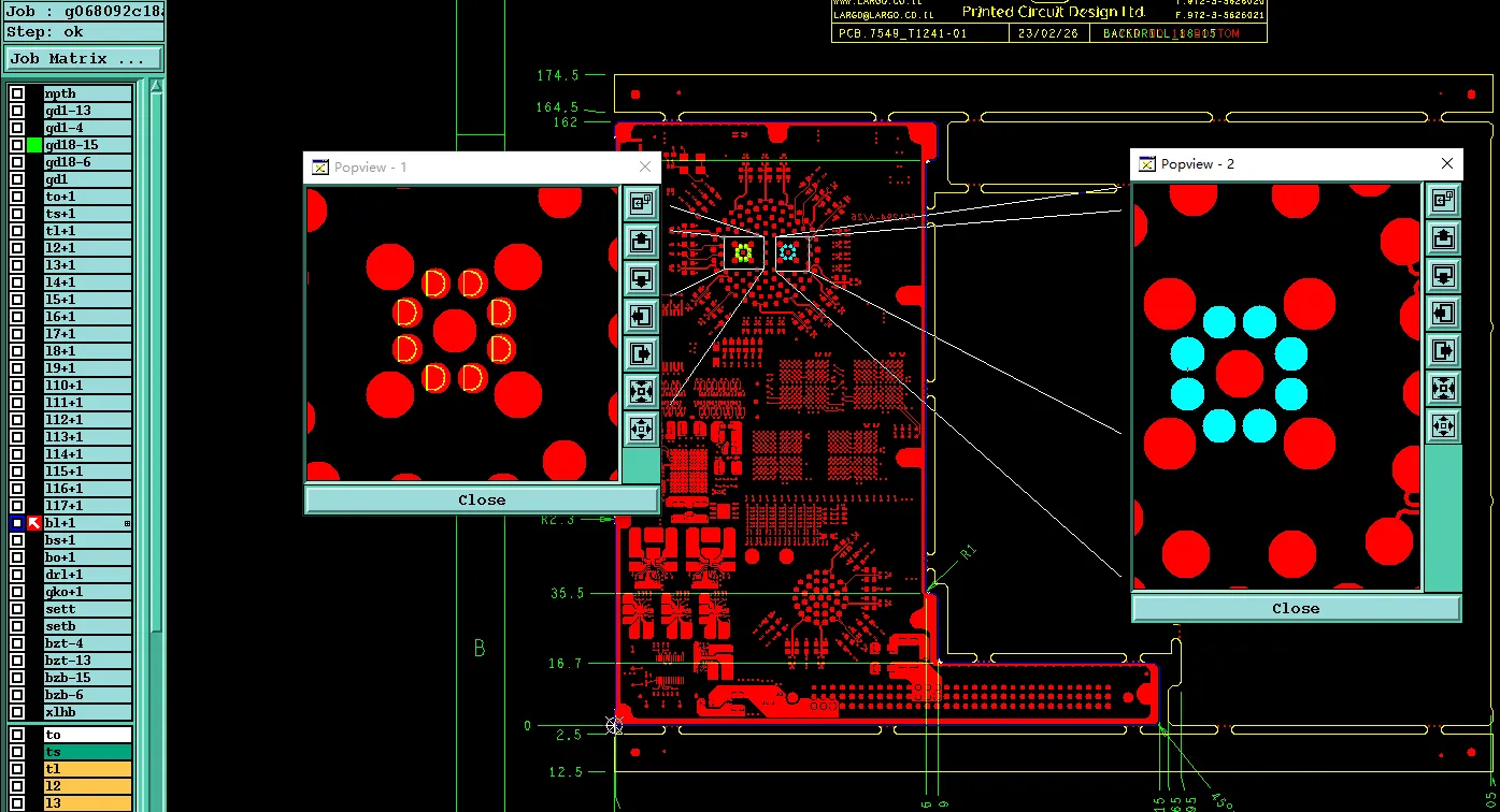
Fixing 18-Layer PCB Risks: The Power of PCB CAM Review
The Impact of Controlled Depth Drilling on High Speed PCB Performance
The Role of Controlled Depth Drilling in RF PCB Design
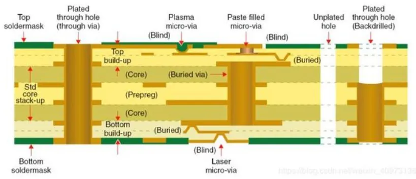
A Deep Dive into PCB Via Stubs and Controlled Depth Drilling Solutions
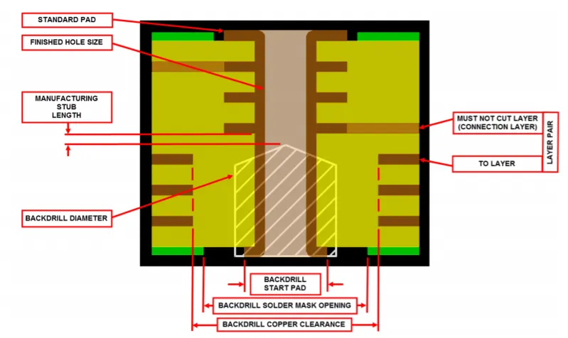
Backdrilling and Blind Vias: A Combined Approach to Signal Integrity
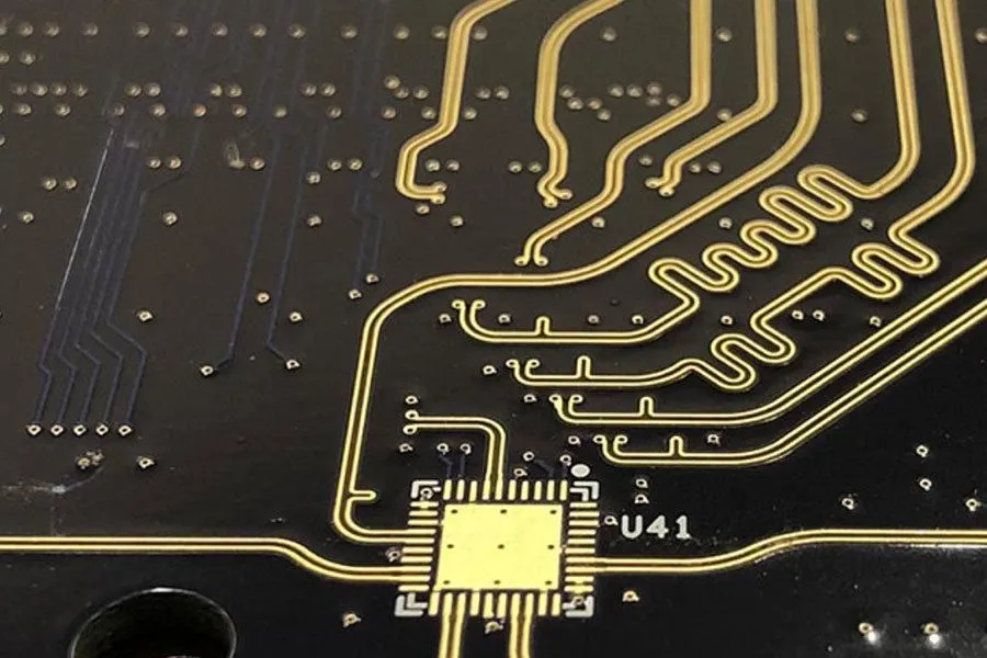
HDI PCB Signal Integrity Design: Key Considerations & Guidelines
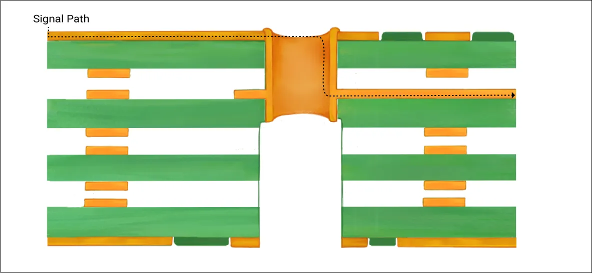
Backdrilling Design: A Beginner's Guide to Reducing Signal Reflections in PCBs
Advanced Backdrilling Design: Optimizing Stackup for High Performance PCBs
Signal Integrity Secrets: How Backdrilling Design Optimizes Your PCB Performance
DIY Controlled Depth Drilling: Build Your Own PCB Signal Booster
PCB Back Drilling: The Key to Unlocking High Frequency Performance
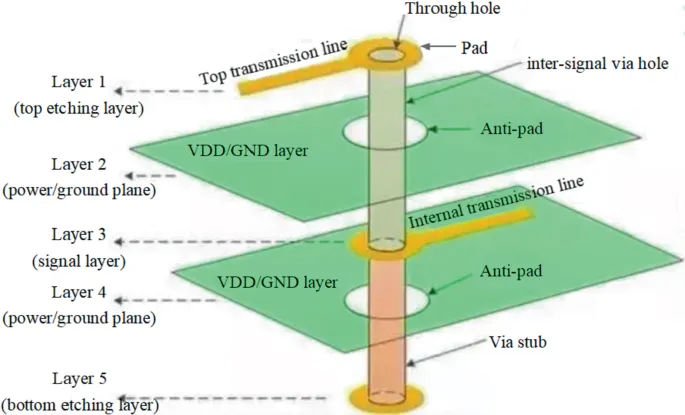
Advanced PCB Back Drilling Techniques for High Speed Digital Circuits
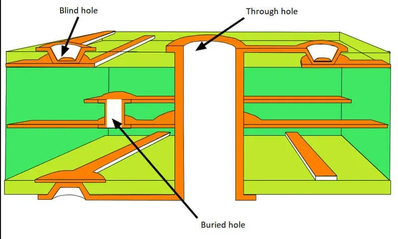
PCB Back Drilling vs. Blind and Buried Vias: Which is Right for Your Design?
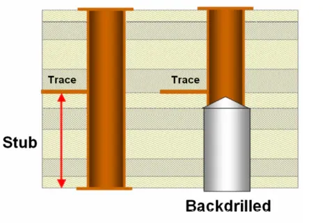
Controlled Depth Drilling for Beginners: A Hobbyist's Guide to PCB Perfection
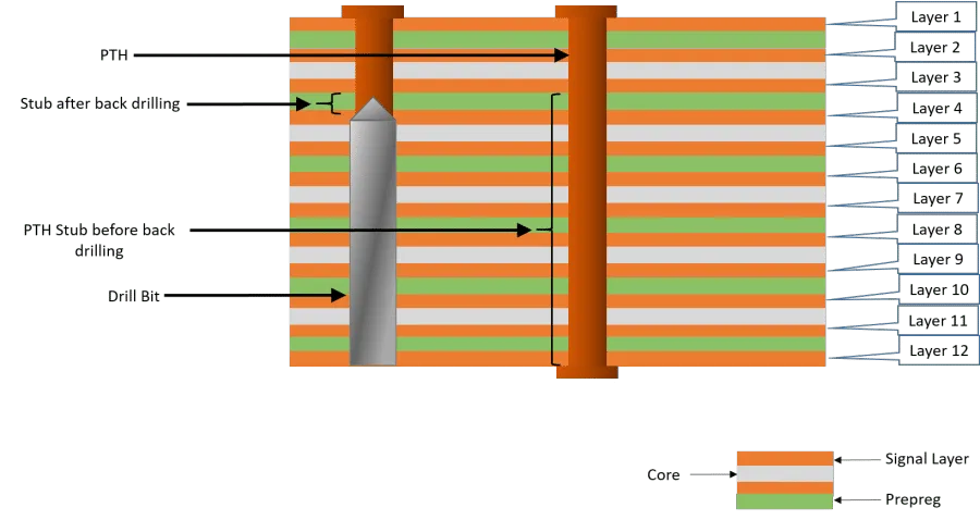
Simulating Backdrilling: How to Optimize PCB Performance Before Manufacturing