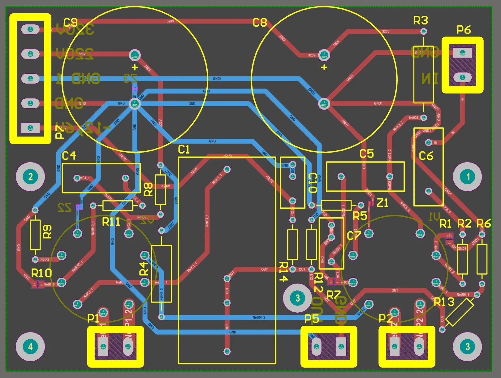
Hardware engineers are used to seeing dense arrays of holes on a PCB. Some of those holes are missing the copper ring that normally surrounds a plated through-hole. The feature looks minor, but padless holes are a key method in high-density PCB design. This article explains what they are, why they are used, and what they cost in reliability and process control.
What Is the Annular Ring on a PCB Hole?
Before padless holes, the starting point is a conventional plated through-hole (PTH). An ordinary PTH is a three-part structure:
- The drilled hole in the board
- The copper plating on the hole wall, which connects copper on different layers
- The pad: the copper ring around the hole. The remaining copper after the hole is subtracted from that pad is the annular ring.
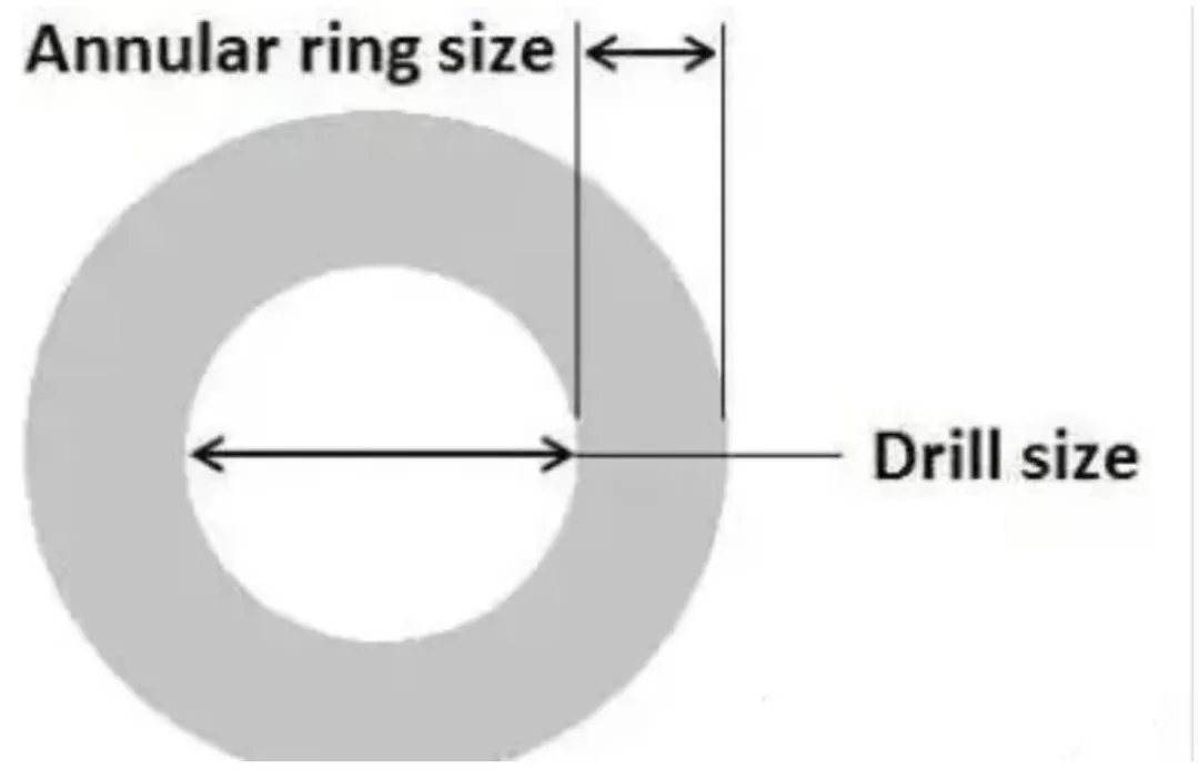
The ring looks small, but it does two jobs. It anchors the barrel copper to the copper on each layer so the connection is less likely to lift under heat or mechanical load. It also provides drill-breakout margin: if the hole is slightly off center, the remaining ring can still keep the electrical connection intact.
Why Remove the Annular Ring?
If the ring is useful, the reason to remove it is still simple: it frees routing space. That matters on phones, computers, and high-end communications products that need smaller size and higher density.
1. Escape Routing Under Fine-Pitch BGAs
The gap between pins on a fine-pitch BGA is very small. A conventional PTH with an annular ring fills that gap, and signal traces cannot escape between the pins. After the ring is removed, a trace can pass close to the hole edge and the routing bottleneck is opened.
2. Reducing Shorts to Metal Housings
Some parts have a metal shell. An exposed annular ring on the PCB can touch that metal during assembly and cause a short. Removing the ring removes that contact path at the source.
A padless PTH is therefore a trade-off: some reliability is given up to gain routing space. Pads are not deleted on every layer. They are removed only on layers that do not need a connection, so traces can use the recovered area.
Padless Holes Are Not One Process
A padless hole is not only "delete the copper ring." Common implementations include:
- Direct padless design: either remove the pad on non-critical layers completely, or make the pad the same diameter as the hole so no extra ring remains.
- Via-in-pad plus plugged and plated hole: drill the via in the center of a BGA pad so the pad itself acts as the ring, then fill the hole with resin and plate it flat. The finished surface looks padless and solder is less likely to wick into the hole.
- Back-drilling: for high-speed signals, drill away the unused portion of the barrel copper. That removes the stub that would otherwise reflect and attenuate the signal, and it also leaves a padless condition on the unused layers.
Benefits and Risks
Benefits
- Higher routing density: this is a core method for high-density interconnect (HDI) and allows more complex routing in a limited layer count.
- More stable signals: via parasitic capacitance is reduced. Back-drilling also lowers reflection and attenuation on high-speed nets and improves signal integrity.
- More inner-layer routing freedom: traces no longer have to avoid unused pads on every layer.
Drawbacks: Tighter Process and Higher Cost
- Lower mechanical reliability: without a pad to anchor the barrel, adhesion between the hole-wall copper and the inner-layer copper is weaker. Cracks or opens are more likely after multiple reflow cycles.
- Higher fabrication demand: layer-to-layer registration and drill accuracy must be very tight. A small offset can cause an open or a short. Plating must also hold barrel thickness and uniformity to offset the lost mechanical strength.
- Cost and inspection: high-accuracy process steps raise manufacturing cost. Conventional AOI also has difficulty judging the connection quality of a padless hole, and later debug and repair are harder.
Summary
Padless holes are not a display of process capability. They are a response to smaller, higher-performance electronics. The ring is not removed at random. The choice depends on the signal path and on whether the fabricator can hold registration, drill, and plating. In communications, computing, and consumer electronics, padless holes are now a common feature of high-end PCB design. The design goal is to recover routing space without letting the reliability risk exceed the gain.
For a high-density PCB, evaluate the fabricator's process capability first, then choose how padless holes will be used. The trade-off is useful only when the routing benefit clearly outweighs the reliability and cost risk.
SEO Title: Padless PTH Holes: Why PCBs Remove the Annular Ring Meta Description: Why high-density PCBs remove annular rings on unused layers for BGA escape routing, plus via-in-pad, back-drilling, HDI density gains, and reliability risks after reflow.