 00:58
00:58
Via Stubs
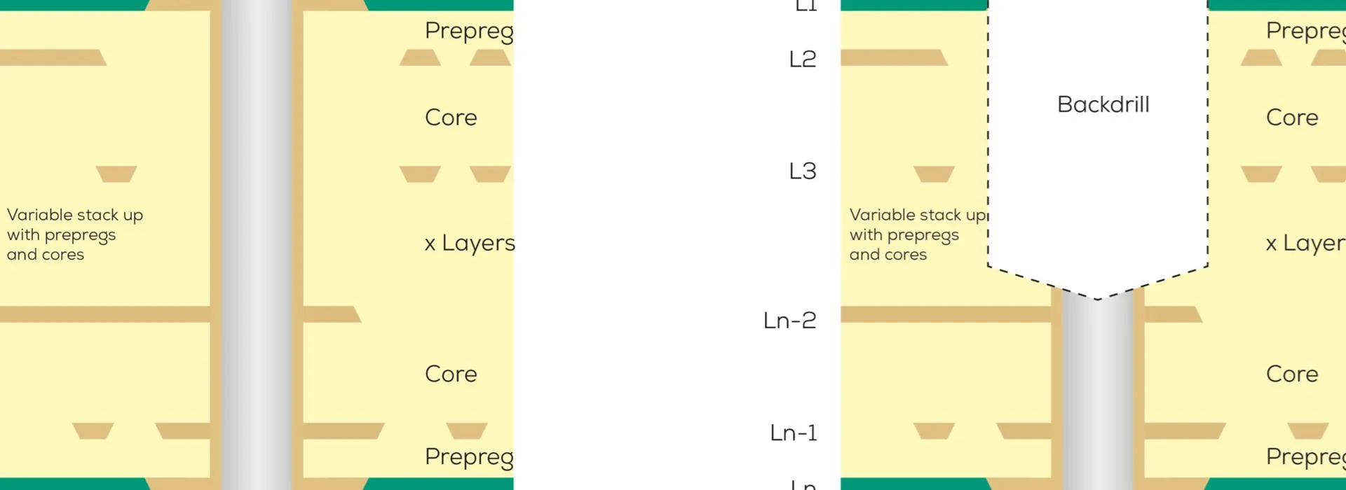
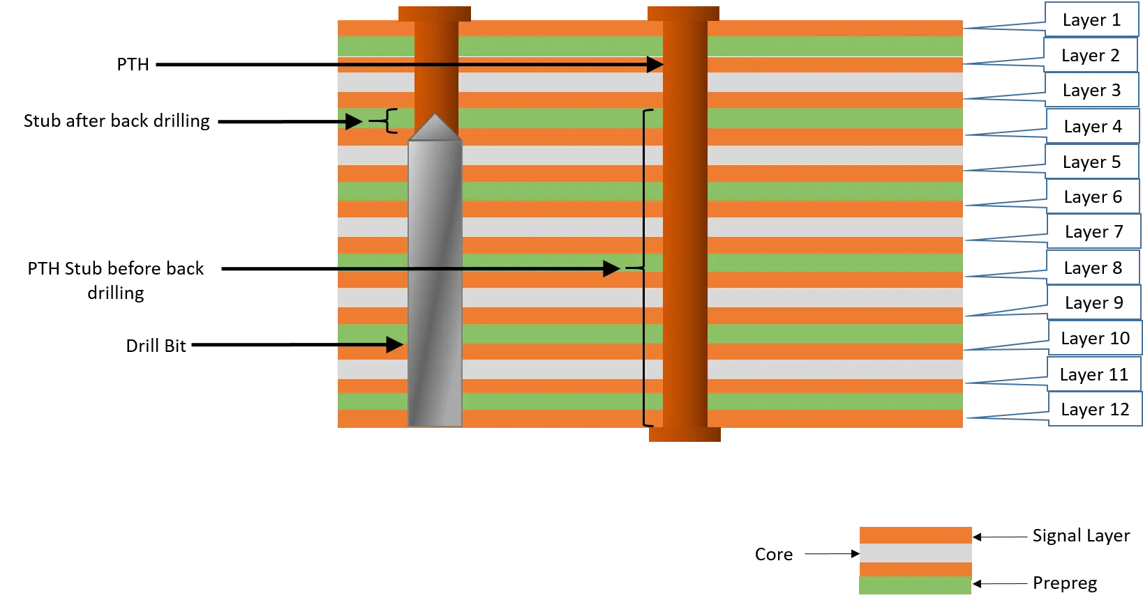
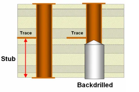
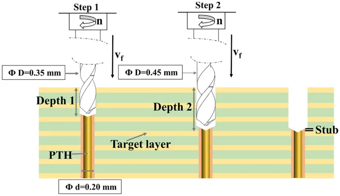
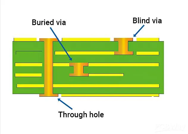
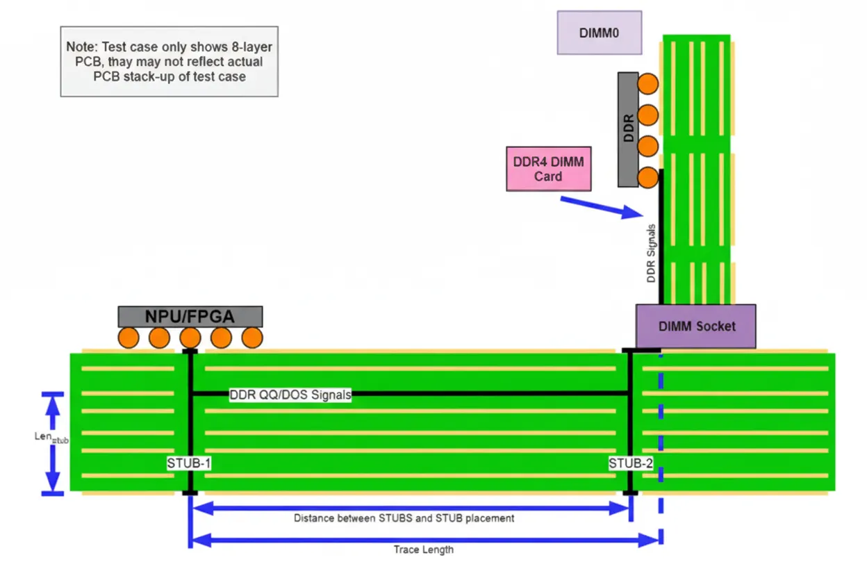
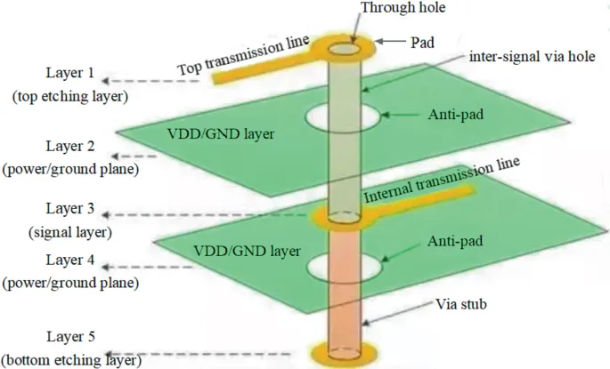
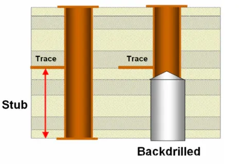
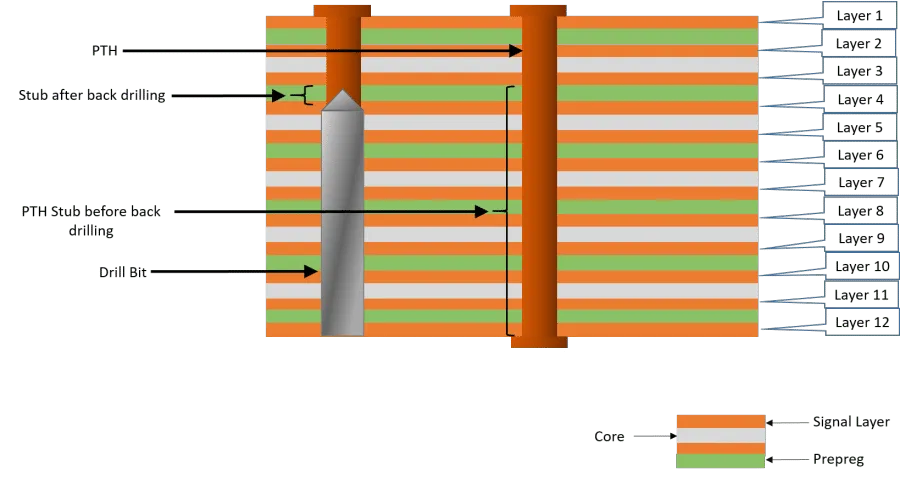
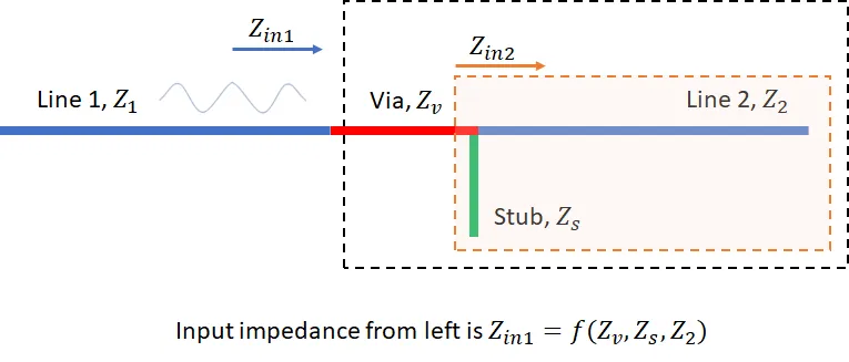
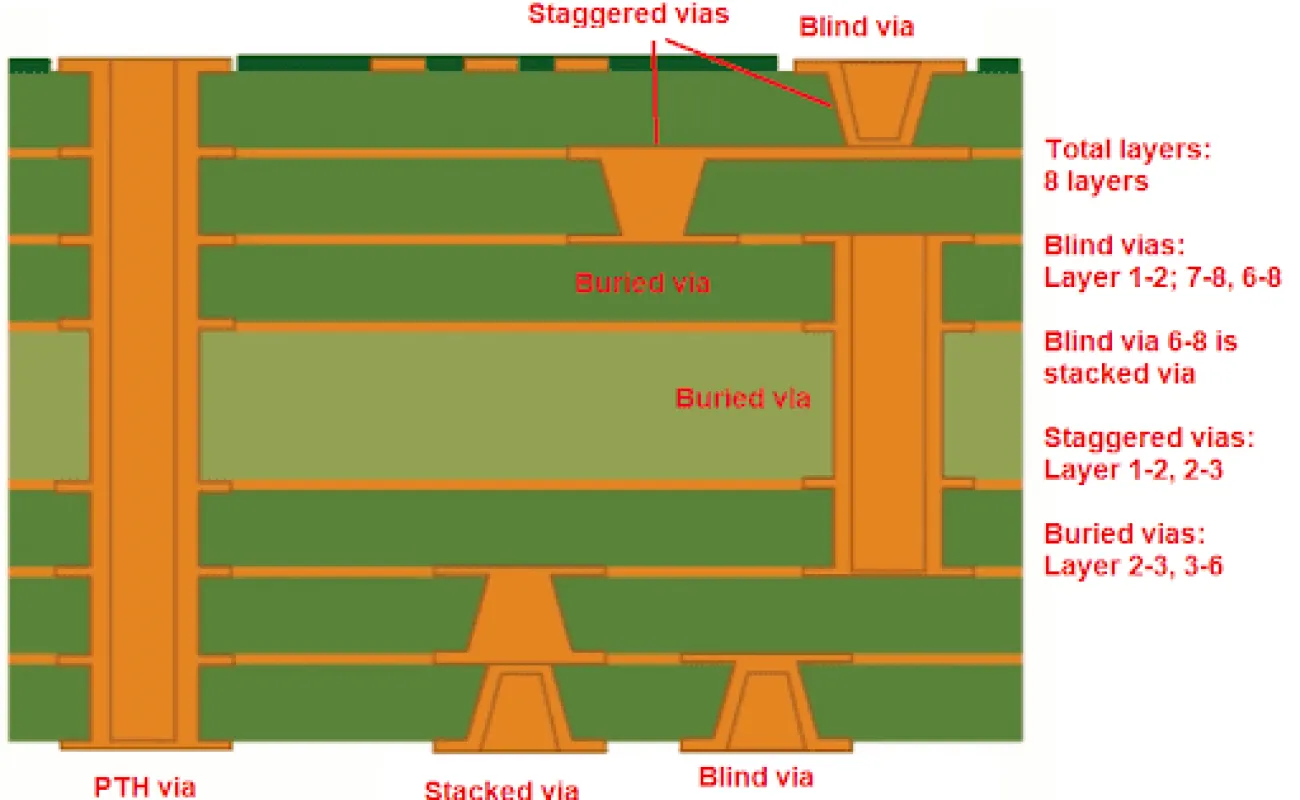
Via stubs represent a critical consideration in printed circuit board (PCB) design, particularly for high-speed and high-frequency applications. In multilayer PCBs, vias connect traces across different layers, but when a via extends beyond the necessary connection point, it creates a stub—a dangling segment of conductive material that does not carry the signal. These via stubs can act as unintended resonators or antennas, leading to signal reflections, impedance discontinuities, and attenuation that degrade overall performance. Engineers searching for information on via stubs often encounter challenges in maintaining signal integrity, especially in designs involving gigabit data rates, RF circuits, or differential signaling, where even small parasitic effects can cause failures. Understanding and mitigating via stubs is essential for optimizing PCB layouts. Common issues include increased insertion loss and crosstalk, which become pronounced at higher frequencies. To address these, designers employ techniques such as backdrilling, where the unused portion of the via is removed to eliminate the stub. Other approaches include using blind or buried vias to avoid stubs altogether, or implementing via-in-pad designs for denser boards. Best practices involve simulating via structures during the design phase using tools like electromagnetic field solvers to predict and minimize stub effects. By carefully selecting via types and layer stacks, you can enhance signal quality, reduce electromagnetic interference, and improve manufacturing yield. The articles tagged under Via Stubs delve into these topics with detailed explanations, case studies, and step-by-step guidance. Whether you are troubleshooting existing designs or planning new ones, reviewing these resources can provide the insights needed to implement effective strategies and avoid common pitfalls in your projects.
Video Guide
-
00:58
Technical Articles
Technical Guide to 18-Layer Mixed-Lamination PCB
Signal-Integrity Simulation: Five Places Designs Usually Break

Why Backdrill Stubs Can Still Be Too Long After the Layer Pair Is Correct
How to Resolve Backdrill, Press-Fit & Copper Balance Issues in 3mm 24-Layer FR4 PCB
The Impact of Controlled Depth Drilling on High Speed PCB Performance
The Role of Controlled Depth Drilling in RF PCB Design
HDI PCB Signal Integrity Design: Key Considerations & Guidelines
Advanced Backdrilling Design: Optimizing Stackup for High Performance PCBs
Signal Integrity Secrets: How Backdrilling Design Optimizes Your PCB Performance
Enhancing PCB Signal Integrity: A Guide to Blind Vias and Anti-Pads
Via Stub Effects on DDR4 Parallel Links
Advanced PCB Back Drilling Techniques for High Speed Digital Circuits
Controlled Depth Drilling for Beginners: A Hobbyist's Guide to PCB Perfection
Simulating Backdrilling: How to Optimize PCB Performance Before Manufacturing
HDI Via Stub Problems: When Do They Actually Affect Signal Performance?
Controlled Depth Drilling vs. Other Via Techniques: Choosing the Right Approach