Introduction
In high-speed PCB designs running at 28 GHz Nyquist frequencies—common in 56 Gbps PAM4 signaling—a via stub as short as 15–20 mils can trigger quarter-wave resonances that close the eye diagram by 20% or more, dramatically increasing bit error rates and risking link failure. These stub-induced reflections create impedance discontinuities, excessive insertion loss, and signal distortion that conventional through-hole vias exacerbate in multilayer boards.
Blind vias combined with carefully engineered anti-pads offer a proven solution for superior PCB signal integrity. By terminating signals on inner layers without unnecessary stubs, blind vias minimize parasitic inductance and capacitance while anti-pads precisely control impedance and reduce unwanted coupling to reference planes. This guide explores the mechanics, design parameters, simulation workflows, real-world performance data, and manufacturing considerations for leveraging blind vias and anti-pads. Whether designing 5G mmWave modules, PCIe 5.0/6.0 interfaces, or aerospace radar systems, mastering these techniques helps engineers achieve consistent 50 Ω impedance, lower reflections, and reliable performance at multi-gigahertz speeds.
What Are Blind Vias and Why Are They Essential for Signal Integrity?
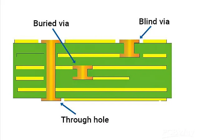
Blind vias represent a specialized type of vertical interconnect in multilayer printed circuit boards (PCBs). Unlike traditional through-hole vias that penetrate all layers, blind vias connect an outer layer to only one or more internal layers, without extending all the way through the board. This characteristic makes them particularly valuable in high-density interconnect (HDI) designs where maximizing board space is crucial.
The primary advantage of blind vias, particularly concerning signal integrity, stems from their ability to shorten signal path lengths. In high-speed circuits, extended signal routes can introduce unwanted delays, signal degradation, and distortion. By allowing signals to traverse shorter distances between layers, blind vias effectively minimize parasitic capacitance and inductance, which helps preserve signal clarity and reduces interference, especially in applications like 5G communication boards operating at gigahertz frequencies.
Related Reading: Unlocking PCB Density: A Beginner's Guide to Blind Vias
Key Considerations for Blind Via Pad Design
The design of the pad for a blind via is fundamental to ensuring robust electrical connections and maintaining signal quality throughout the PCB. The pad is the conductive area where the via terminates, connecting to traces or components. Inadequate pad design can lead to signal reflections or mechanical stress during the manufacturing process.
Pad Dimensions and Form
The dimensions of the blind via pad must be precisely calculated, taking into account the via's drill diameter and the specific manufacturing processes involved. A general guideline suggests the pad diameter should be at least 1.5 times the drill diameter to facilitate proper plating and ensure a reliable connection. For instance, a 0.2 mm drill might require a 0.3 mm pad. A circular pad shape is commonly preferred due to its ability to distribute stress uniformly during drilling and plating operations.
Understanding Aspect Ratio
The aspect ratio, defined as the ratio of the via's depth to its diameter, is another critical design parameter. For blind vias, a lower aspect ratio (ideally less than 1:1) is desirable. This ensures uniform copper deposition during plating, which is vital for electrical reliability and preventing signal loss. High aspect ratios can result in uneven plating, leading to impedance mismatches that negatively impact signal integrity.
Strategic Placement and Routing
Strategic placement of blind via pads is essential to prevent interference with adjacent traces or components. In high-speed applications, position the via as close as possible to its signal source or destination. This minimizes "stub effects"—unused portions of the via that can act as antennas, causing signal reflections. Furthermore, routing signals through blind vias in a controlled manner helps maintain consistent impedance, often targeting a 50-ohm characteristic impedance for high-frequency circuits.
What Is an Anti-Pad and How Does It Influence Signal Integrity?
An anti-pad, also known as a clearance pad, is a non-conductive area or void intentionally created around a via on an internal plane layer of a PCB. Its fundamental purpose is to isolate the via from unintended electrical contact with the surrounding conductive plane (such as a ground or power plane) while precisely controlling the via structure's impedance. In high-speed designs, anti-pads are indispensable for preserving signal integrity.
Without an anti-pad, a via passing through a power or ground plane could inadvertently create a short circuit or introduce excessive parasitic capacitance. This would severely disrupt signal transmission. By carefully dimensioning the anti-pad, engineers can fine-tune the via's impedance to match the impedance of the connecting traces, thereby minimizing signal reflections and ensuring clean, uninterrupted signal flow. For example, in a system designed for a 50-ohm impedance, the anti-pad size can be adjusted to maintain this value precisely.
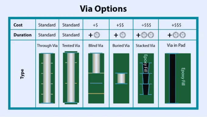
Blind, Buried, and Through-Hole Vias: Detailed SI Comparison
Different via topologies offer trade-offs in signal integrity, density, and cost. The table below summarizes key parameters for high-speed applications (>10 GHz):
| Via Type | Typical Stub Length | Parasitic Inductance | Parasitic Capacitance | SI Performance (@ 28 GHz) | Relative Cost | Best Use Case |
|---|---|---|---|---|---|---|
| Blind Via | Minimal (layer-specific) | 0.3–0.6 nH | 0.1–0.3 pF | Excellent (low reflection, <0.3 dB loss/transition) | Medium-High | HDI, 5G, PCIe high-speed layers |
| Buried Via | None (internal only) | 0.4–0.7 nH | 0.15–0.35 pF | Very Good | High | Inner-layer routing in dense HDI |
| Through-Hole | Full board thickness (can be backdrilled) | 1.0–2.5 nH | 0.4–0.8 pF | Poor without mitigation; improved with backdrilling | Low | Low-layer count, cost-sensitive designs |
| Backdrilled Through | <15 mil remnant | 0.6–1.0 nH | 0.3–0.5 pF | Good (cost-effective stub reduction) | Medium | High-volume servers, where blind vias are cost-prohibitive |
Backdrilling remains a popular, lower-cost alternative to blind vias for stub removal. It mechanically drills out the unused portion of a through-hole via after plating, typically leaving a 10–15 mil stub. While not as clean as a true blind via, backdrilling can recover 70–80% of the SI performance at a fraction of the cost for boards with fewer layers. Choose blind vias when density, layer count, or ultimate performance at 28 GHz+ justifies the premium.
Best Practices for Blind Via Anti-Pad Design
Optimizing the design of blind via anti-pads is crucial for maximizing signal performance in multilayer PCBs. Adhering to specific best practices can significantly enhance overall circuit reliability.
Determining Optimal Anti-Pad Size
The correct anti-pad size is contingent on several factors, including the via diameter, the PCB layer stack-up, and the target impedance. A common guideline suggests an anti-pad diameter that is 2 to 3 times the via drill diameter. For a 0.2 mm via, an anti-pad between 0.4 mm and 0.6 mm might be appropriate. However, for critical high-speed designs (e.g., lines operating at 10 GHz), electromagnetic simulation tools provide the most accurate values by modeling the complex interaction between the via and the plane.
Customizing for Specific Layers
In complex multilayer PCBs, different internal planes may require varying anti-pad sizes based on their specific function (e.g., dedicated ground planes versus power planes). For blind vias that only traverse a limited number of layers, it is important to apply anti-pads exclusively to the relevant planes. This prevents introducing unnecessary capacitance or inductance on layers where isolation is not required or where the via does not make contact.
Mitigating Capacitive Coupling
Excessive capacitive coupling between a via and its surrounding plane can significantly degrade signal integrity, particularly by slowing down signal rise times in circuits operating above 1 GHz. A properly designed anti-pad increases the physical separation between the via barrel and the plane, thereby reducing this unwanted coupling. Utilizing PCB design software for simulation allows engineers to adjust anti-pad dimensions to minimize coupling effects and optimize signal performance.
General PCB Design Guidelines for Vias and Signal Integrity
Beyond the specific considerations for blind via pads and anti-pads, a broader set of best practices for via design is crucial for enhancing signal integrity. These guidelines are applicable to all via types and are particularly vital in high-speed and HDI applications.
Implementing Controlled Impedance Routing
Maintaining consistent impedance across the entire signal path, including through vias, is paramount for high-speed signals. Even small impedance mismatches, as little as 5 ohms, can cause significant signal reflections. Employing simulation tools to match the impedance of traces, vias, and pads—adjusting anti-pad sizes and via dimensions as necessary—is a key practice. For deeper guidance on achieving consistent impedance across layers, see our guide to optimizing PCB stack up for high speed signals.
Optimizing Via Placement
Vias should be positioned carefully, away from sensitive analog components or high-speed digital traces, to prevent crosstalk. If multiple vias are required, staggering their placement can help reduce electromagnetic interference (EMI). In HDI designs, blind vias inherently save space, allowing for tighter component placement without compromising signal quality.
Related Reading: Blind Vias in PCB Design: Optimizing High-Density Boards
Incorporating Robust Ground Planes
A continuous, solid ground plane situated near signal layers provides an essential low-impedance return path for high-frequency signals, thereby minimizing noise and EMI. It is crucial to ensure that blind vias have nearby ground vias to maintain this return path, particularly in designs operating above 500 MHz.
Minimizing Via Stubs
Via stubs, which are unused portions of a via, can act as resonant structures that distort high-speed signals. While blind vias inherently mitigate this issue by not extending through the entire board, precise design of the via depth is still important to avoid any unnecessary length that could behave as a stub.
Comprehensive Simulation and Testing
Prior to finalizing a PCB layout, it is imperative to use simulation software to model signal behavior through blind vias and anti-pads. These tools can predict potential issues such as signal reflection, crosstalk, and impedance mismatches, enabling early design adjustments. Post-manufacturing, using a time-domain reflectometer (TDR) to verify impedance values, typically targeting a ±10% tolerance for critical signals, confirms design integrity.
Overcoming Challenges in Blind Via and Anti-Pad Design
Designing blind vias and anti-pads for optimal signal integrity presents several challenges, particularly in the context of complex multilayer boards. Awareness of these common issues and their solutions is crucial.
Addressing Manufacturing Limitations
Blind vias demand highly precise drilling and plating processes, often utilizing laser technology for microvias in HDI boards. If the aspect ratio is too high, plating failures can occur, leading to open circuits.
Solution: Collaborate closely with your PCB manufacturer to understand their specific capabilities and design within those limits, generally keeping aspect ratios below 1:1.
Mitigating Impedance Mismatches
Even minor deviations in anti-pad size or via dimensions can lead to impedance mismatches, resulting in detrimental signal reflections.
Solution: Employ simulation tools to precisely fine-tune anti-pad and pad dimensions, ensuring a consistent target impedance (e.g., 50 ohms) throughout the entire signal path.
Managing Signal Crosstalk
In densely packed layouts, signals passing through adjacent vias can interfere with one another, degrading overall performance.
Solution: Ensure adequate spacing between vias and strategically incorporate ground vias to shield high-speed signals. A general guideline is to maintain a separation of at least three times the via diameter between critical signals.
Real-World Case Studies and Test Data
In a 5G mmWave small-cell module operating at 28 GHz, replacing through-hole vias with laser-drilled blind vias and optimized 0.5 mm anti-pads reduced per-transition insertion loss from 0.8 dB to 0.3 dB. Eye height improved by 25% at 28 Gbps, meeting stringent BER targets while shrinking board area by 18%.
A PCIe 5.0 (32 GT/s) server motherboard implementation used via-in-pad blind vias with 30–35 mil round anti-pads and per-layer backdrilling. Measured return loss stayed below –15 dB to 16 GHz, and differential crosstalk remained under –40 dB. The design passed full compliance testing on the first silicon spin, avoiding costly respins.
In an aerospace radar system, blind vias combined with tight ground stitching reduced via-to-via crosstalk by 12 dB in a dense 18-layer stack-up, ensuring clean signal integrity for phased-array beamforming at X-band frequencies. These examples demonstrate quantifiable gains when blind vias and anti-pads are designed with simulation-backed precision.
Manufacturing Considerations, DFM, and Common Pitfalls
Blind vias require laser drilling for microvias (<0.15 mm) and precise registration (±50 µm or better). Aspect ratios above 1:1 frequently cause plating voids—keep them ≤ 0.8:1. Material selection matters: low-Dk, low-Df laminates improve performance but can complicate lamination cycles.
DFM best practices include:
- Early fabricator engagement to align on minimum via size, anti-pad clearance, and aspect ratio capabilities.
- Specifying copper roughness (VLP or RTF) and providing full stack-up drawings with impedance targets.
- Adding test coupons for TDR verification and cross-section analysis.
- Avoiding square anti-pads that create resonant cavities.
Common pitfalls are mismatched anti-pad sizes across layers, insufficient ground stitching, and ignoring etch factor compensation in trace width calculations. Collaboration with an experienced manufacturer typically prevents these issues and ensures ±10% impedance tolerance on critical nets.
Future Trends in HDI and High-Speed Signal Integrity
As data rates push toward 224G SerDes (112 GHz Nyquist), microvias with diameters <0.1 mm and stacked via structures will become standard. These ultra-short interconnects further minimize stub effects and parasitic reactance required for clean signaling.
AI-driven EDA tools are emerging that automatically optimize via placement, anti-pad geometry, and return via arrays using machine learning trained on vast simulation datasets. Hybrid approaches combining blind microvias on outer layers with buried vias internally will dominate next-generation 5G-Advanced, 6G, and AI accelerator boards.
Expect tighter integration with embedded waveguide structures and glass-core substrates to reduce loss further. Designers who master today's blind via and anti-pad techniques will be well-positioned for these evolving high-speed challenges.
Concluding Thoughts: Optimizing PCB Performance with Intelligent Via Design
Mastering the design of blind via pads and anti-pads is indispensable for achieving high signal integrity in modern PCB layouts, especially for high-speed and high-density electronic applications. By meticulously considering pad sizes, anti-pad dimensions, impedance control, and strategic via placement, engineers can effectively minimize signal loss, reduce electromagnetic noise, and ensure robust, reliable performance. Adhering to comprehensive PCB design best practices for vias, from controlled impedance routing to thorough simulation and post-manufacturing testing, further elevates the quality of the final product.
At AIVON, we recognize the critical importance of precision in both PCB design and fabrication. By applying the principles detailed in this guide, designers can create circuits that meet the demanding requirements of contemporary electronic systems, whether for telecommunications, computing, or consumer devices. With a well-informed approach, blind vias and anti-pads transform into powerful tools for maintaining signal integrity and optimizing overall board performance


