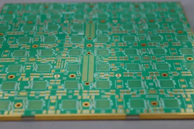
This article analyzes an 18-layer complex printed circuit board that integrates multistep blind vias, selective backdrilling, sintered copper paste vertical interconnects, vacuum resin via fill for via-in-pad, edge plating, embedded resistors, and internal blind cavities. It breaks down the major manufacturing challenges, details key controls for each special process, and provides technical guidance for high-frequency, high-speed, and high-reliability applications such as communications, radar sensing, industrial control, aerospace subsystems, and high-power supplies.
Special Process Highlights
1. Multistep segmented blind vias (L1–L10, L11–L14, L15–L18)
Process flow: Three sub-boards are independently laminated, drilled, plated (electroless copper plus panel plating), resin-filled, and planarized. After all sub-boards are prepared, a final lamination bonds them into the full stack-up, achieving segmented blind-via interconnects across sub-boards.
Engineering value: This approach distributes BGA layer-transition paths, shortens high-speed signal routes, reduces loss and crosstalk, and frees surface routing resources.
Key controls: Minimum drilled diameter per sub-board is 0.25 mm. Perform plasma desmear prior to plating to ensure reliable metallization. After resin via fill, grinding/planarization is mandatory; boards that fail planarity must not enter the etching process.
2. Selective backdrill (L1–L12, L1–L13)
Targets: Two theoretical backdrill depths of 0.17 ± 0.05 mm and 0.07 ± 0.05 mm are used, with finished via stub strictly controlled to 0.08–0.12 mm. The backdrill must not damage the target internal copper layers L12 or L13.
Engineering value: Removing via stubs suppresses high-speed resonance and reflections, improving eye-diagram quality and helping the link meet high-frequency/high-speed performance requirements.
Key controls: Perform first-article cross-section analysis to verify stub depth prior to volume production. Implement closed-loop drill-depth monitoring and compensate for board thickness tolerance to keep backdrill within the narrow window.
3. Sintered copper paste vertical interconnects (L1–L11, L11–L18, L14–L18)
Engineering value: Compared with plated blind vias, sintered copper paste interconnects provide lower resistivity and superior vertical thermal conductivity, enabling both high-quality signal interconnects and robust heat-conduction paths for power dissipation.
Key controls: Control the sintering atmosphere to prevent oxidation of the copper paste. Manage the sintering–lamination thermal cycles to mitigate CTE mismatch between copper paste and base materials, avoiding delamination and interfacial voids. After sintering, grind and planarize to ensure adequate adhesion for subsequent trace formation.
4. Vacuum resin via fill
Application: Fill blind and buried vias in sub-boards to realize via-in-pad structures, eliminate surface recesses, reduce solder voiding risk, and increase routing density.
Key controls: Use vacuum via fill, then cure and grind. Perform 100% inspection of via-fill quality. If post-fill planarity does not meet specification, the panel must not proceed to etching. The manufacturing instruction (MI) defines responsibility and traceability.
5. Embedded resistors on L12
Engineering value: Embedding passive components in internal layers reduces the number of SMT devices, lowers high-frequency parasitic inductance, and saves board space. This is well suited to RF attenuation networks and precision sampling circuits.
Key controls: Tight control of resistive film thickness uniformity is required. Manage etch and lamination effects that can cause resistance drift. Verify resistance values on the first article.
6. Internal blind cavity (controlled-depth milled stepped slot) on L15–L18
Targets: Bottom-side controlled-depth milling to a depth of 1.2 mm with a tolerance of ±0.1 mm. Do not damage the L14 copper foil.
Engineering value: Creates an internal cavity for embedded devices or an air dielectric region to optimize RF performance.
Key controls: Lock controlled-depth milling parameters. Perform first-article cross-sections to confirm the condition of the cavity floor and edges. Prevent copper foil lifting and resin-starved delamination.
7. Edge plating and unique serial marking
1) Edge plating (metal edge): Improves board-edge mechanical strength, reduces the risk of edge chipping and copper foil lift during assembly, and provides ancillary EMI shielding benefits.
2) Unique serial number: Incremental serialization supports full lifecycle traceability required by high-reliability products.
8. Surface finish and reliability testing
ENIG (immersion gold over electroless nickel) provides reliable performance for multiple soldering cycles and high-frequency contact. Completed boards undergo flying-probe electrical testing and 100% FQC/FQA. Cross-section and outgoing inspection reports are provided per lot.
Core Manufacturing Challenges
1. Mixed-Tg lamination stress and registration risk
The stack-up combines three base materials (Tg 280 °C, Tg 180 °C, and Tg 170 °C) and uses three sub-laminations plus one final lamination. Multiple high-temperature cycles accumulate stress and can cause board warp, interlayer shift, and inner-layer microcracks. Each lamination cycle must tightly control panel thickness tolerance to ±0.08 mm.
2. Narrow backdrill depth window
Backdrill stop layers for L1–L12 and L1–L13 are separated by only one layer, with a finished stub window of 0.08–0.12 mm. Excess depth risks damaging the internal copper; insufficient depth leaves stubs that degrade high-speed performance. First-article cross-section confirmation is mandatory.
3. Cascading risk from resin via-fill planarity
Multiple downstream processes depend on surface planarity after resin via fill. The MI explicitly prohibits etching if planarity is out of spec; otherwise, open circuits and impedance drift can occur.
4. Narrow process window for copper paste sintering
High-temperature sintering is prone to oxidation. CTE mismatch between copper paste and dielectric can generate interfacial gaps or changes that manifest as impedance drift during thermal cycling. Post-sinter planarity and surface condition also affect the yield of subsequent fine-line imaging and etching.
5. Embedded resistor value stability
Etch bias and resin flow during lamination can change the resistor geometry and resistance. Continuous engineering oversight and first-article resistance validation are required to maintain specification.
6. Controlled-depth internal blind cavity risk
With a ±0.1 mm milling tolerance, any overcut can directly damage the functional copper on L14. Resin starvation or localized delamination is more likely in cavity regions during lamination and must be prevented through parameter control and inspection.
Process Assurance Measures
1. Front-loaded engineering evaluation
At the MI stage, complete stack-up simulation and artwork scale compensation (shrink/expansion). Assign dedicated engineering oversight for each special process, with mandatory first-article confirmations at critical steps.
2. Lamination control
Customize stage-wise heating profiles for each lamination cycle. Use X-ray target alignment to monitor interlayer registration. Control finished thickness to ±0.08 mm per lamination to reduce bow and layer-to-layer offset.
3. Control of critical hole processes
Backdrills, sintered copper paste vias, and resin-filled vias all require first-article cross-section verification. Implement online depth monitoring and closed-loop adjustments in mass production.
4. Mandatory gates for special processes
If resin-fill planarity, embedded-resistor values, or blind-cavity depth do not meet specification, the panel must not proceed to the next process. Enforce process accountability and corrective action before release.
Target Applications
High-complexity mixed-lamination PCBs of this type target customers and systems with stringent requirements for signal integrity, thermal performance, and reliability, including:
- Radar sensing and satellite-communication RF hardware
- High-speed data transmission equipment
- High-reliability industrial high-power controllers
- Research-institute development projects
- High-end measurement and control equipment
When building first articles for boards that combine multistep blind vias, selective backdrilling, sintered copper paste interconnects, embedded resistors, and internal blind cavities, teams sometimes underestimate the manufacturing complexity. Insufficient process capability or lack of practical experience can lead to repeated prototype failures, project delays, and higher development costs. The engineering controls and process assurance measures outlined above help mitigate these risks and accelerate a smooth path from prototype to stable volume production.