










Press-fit assembly offers solderless, high-reliability, and field-repairable interconnects, and is widely used in telecom equipment, automotive electronics, power modules, and other high-speed signal applications. Unlike wave soldering, press-fit relies on mechanical interference: a compliant (eye-of-the-needle) pin is pressed into a PCB plated through hole (PTH) to create a tight, gas-tight "cold" connection through elastic deformation and contact pressure.
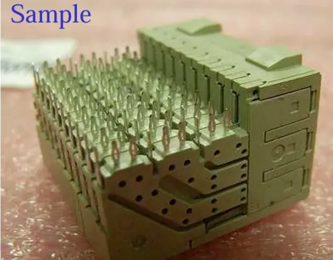
Figure 1 | Press-fit insertion of a compliant (eye-of-the-needle) pin into a plated through hole (PTH)
To achieve reliable press-fit joints, PCB hole design, hole tolerance, copper plating thickness, layer routing strategy, and the keep-out plan around the press-fit area are all critical. The following guidelines consolidate key design and process points to help manufacturing and SMT process engineers get press-fit right the first time.
1. Drill Size and Plated Copper Thickness: Design Essentials
The core of a press-fit joint is the interference fit between the pin and the hole wall. If the finished hole is too large, contact resistance increases and retention force drops; if it is too small, the pin or via barrel can be damaged during insertion. To avoid these failure modes, specify both the drilled diameter and the target finished hole size (after plating), and control the PTH copper thickness.
Always provide both the drill size and the finished hole size to the PCB fabricator. Do not specify the finished hole only.
1.1 Required barrel copper thickness
-
PTH copper thickness: The average or any single-point barrel copper thickness must be ≥ 1 mil (≈ 25.4 μm).
-
Thin barrel copper is prone to cracking during insertion, which can lead to open circuits.
1.2 Drill diameter calculation
First define the allowable finished-hole limits from the connector or device datasheet:
-
Finish hole size (Min): the minimum finished-hole diameter that still meets the pin's fit requirements.
-
Finish hole size (Max): the maximum finished-hole diameter allowed for the pin.
Calculate the drill size using:
Drill size = (Finish hole size (Min) + Finish hole size (Max)) / 2
The calculated drill size must also satisfy both constraints below:
-
Drill size ≥ Finish hole size (Min) + 2 mils
-
Drill size ≤ Finish hole size (Max) – 1 mil
Example: If a part specifies a finished-hole range of 38–42 mil, then Drill size = (38 + 42) / 2 = 40 mil. Check: 40 ≥ 38 + 2 = 40; and 40 ≤ 42 – 1 = 41, both satisfied.
This method yields a drill size that, with approximately 1 mil of barrel copper plating, places the finished hole within the mid-range of the part's allowable window—neither too tight nor too loose—improving insertion yield and contact reliability.
2. Routing to Prevent Trace Damage Near Press-Fit Pins
Press-fit pins typically have a pin shoulder near the PCB surface—a non-insertion section with a larger diameter than the compliant zone. After insertion, the shoulder sits against or slightly indents the PCB surface. Any outer-layer trace within this shoulder footprint is at risk of being crushed or sheared during pressing. Apply the following rules:
2.1 Baseline rule
Avoid any traces on the Top and Bottom layers within the pin shoulder region around the PTH.
2.2 If routing is unavoidable, meet both conditions
-
Orient traces parallel to the shoulder edge profile, not perpendicular.
-
Never run traces underneath the shoulder. Routing that passes beneath the shoulder will be crushed during insertion.
Correct vs. incorrect routing near a pin shoulder:
Correct: Traces parallel to the shoulder contour.
Incorrect: Traces perpendicular to or crossing beneath the shoulder region.
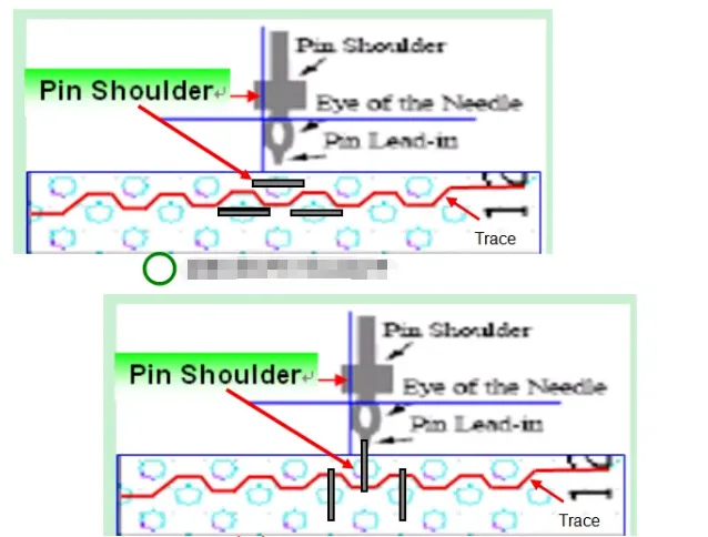
Figure 2 | Correct (left, traces parallel to the shoulder) and incorrect (right, traces perpendicular and crossing under the shoulder) routing practices
In practice, it is recommended to fan out signals to inner layers in the press-fit zone, or maintain at least 1 mm clearance between any outer-layer trace and the shoulder region.
3. Press-Fit Component Keep-Out Zones
To ensure proper tooling access for press equipment (fixtures, support plate, and ram) and to prevent adjacent components from experiencing mechanical stress or interference, observe the following keep-out guidelines.
3.1 Support-side keep-out (typically the PCB back side)
-
No components within 200 mil (5 mm) around the press-fit area.
-
Rationale: The back side requires a flat support surface during pressing. Any protruding component leads to uneven loading or damage.
3.2 Non-support side keep-out (typically the PCB front side)
-
No components taller than 2 mm within 200 mil (5 mm) around the press-fit area.
-
Low-profile passives (e.g., 0402/0201) may be placed if height ≤ 2 mm.
-
Rationale: Provides ram clearance and avoids collision with tall parts.
3.3 Sensitive-component keep-out (both sides)
-
No BGAs, CSPs, or wave-soldered through-hole parts within 400 mil (10 mm) of the press-fit area.
-
BGAs/CSPs are highly sensitive to mechanical stress; local bending or vibration during pressing can crack solder balls.
-
Wave-solder through-hole joints (e.g., DIP connectors) are not designed to absorb press-insertion loads.
If a PCB uses both press-fit connectors and BGAs, keep them at least 10 mm apart and, where possible, place them in different board regions.
DFM Checklist Summary
| Check Item | Requirement |
|---|---|
| Barrel copper thickness | ≥ 1 mil (average or single-point) |
| Drill size calculation | (Min finished hole + Max finished hole) / 2, and satisfy boundary constraints |
| Top/Bottom routing rule | Avoid outer-layer traces; if unavoidable, route parallel to the shoulder and never under the shoulder |
| Back-side keep-out (support side) | No components within 200 mil (5 mm) |
| Front-side keep-out (non-support side) | No components taller than 2 mm within 200 mil (5 mm) |
| Sensitive components (BGA/CSP/wave-soldered THT) | Prohibited within 400 mil (10 mm) on both sides |
Applying the Rules: Practical Workflow
-
Align with the PCB fabricator: Provide the finished-hole tolerance window from the component datasheet. The fabricator should calculate the drill size using the formula and control the PTH copper thickness accordingly.
-
Design review focus: In the press-fit region, verify that outer-layer routing, copper pours, and solder-mask openings comply with the "no trace under the shoulder" rule.
-
Layout planning: Place press-fit parts near board edges or open areas and reserve the keep-out zones. Keep BGAs and other sensitive devices at least 10 mm away.
-
Manufacturability analysis: For dense multilayer boards, consider finite element analysis to estimate board bending and barrel stress during pressing, and adjust support strategy or keep-outs as needed.
Press-fit is not traditional soldering; its design philosophy is mechanics first, electrical follows. Adhering to hole-size tolerances, shoulder clearances, and keep-out rules is essential to achieve a durable, low-resistance, and high-reliability press-fit connection over product lifetime.
Reference: IPC-9797, Acceptability Requirements for Press-Fit Solderless Connections. Additional constraints may apply for different pin types (e.g., eye-of-the-needle vs. solid pins); always follow the component's datasheet.






