Introduction
Surface Mount Technology (SMT) has transformed the electronics industry by enabling the production of compact, high-performance devices. At the heart of SMT lies the PCB assembly process, where precision and reliability are paramount. SMT testing plays a critical role in ensuring that assembled printed circuit boards meet stringent quality standards. For electrical engineers, understanding SMT testing methods is essential to identify SMT defects, verify component integrity, and maintain product reliability. This article explores the intricacies of the SMT testing process within the PCB assembly workflow. It covers the technical principles, common testing methods, a step-by-step breakdown of testing stages, and the relevance of industry standards. By delving into these aspects, engineers can enhance their knowledge of SMT testing and apply best practices to achieve defect-free assemblies.
What is SMT Testing and Why is the SMT Testing Process Crucial?
SMT testing refers to a series of evaluation methods used during and after the SMT PCB assembly process to verify the quality and functionality of the board. These tests focus on detecting SMT defects such as misaligned components, soldering issues, or electrical failures. They also ensure component integrity by confirming that each part operates as intended under specified conditions.
The SMT testing process is vital because even minor defects can lead to system failures, costly rework, or product recalls. With the increasing complexity of electronic devices, the demand for robust SMT testing has grown. Effective testing not only prevents failures but also upholds reliability in applications ranging from consumer electronics to aerospace systems. By identifying issues early across the entire SMT assembly workflow, the SMT testing process saves time and resources while ensuring compliance with industry benchmarks.
Technical Principles of SMT Testing
SMT testing operates on the principle of validating both the physical and electrical characteristics of a PCB after assembly. The primary goal is to detect defects that could compromise performance. These defects often include solder joint failures, component misalignment, or insufficient electrical connectivity. Testing methods are designed to assess different aspects of the assembly process. For instance, visual inspections focus on surface-level issues, while electrical tests verify circuit functionality.
Industry standards such as IPC-A-610H, which defines acceptability criteria for electronic assemblies, guide these evaluations. Another key principle is the correlation between testing and design for testability (DFT). Boards designed with accessible test points facilitate more accurate and efficient SMT testing. Understanding these principles helps engineers select the appropriate testing method for specific assembly challenges.
Common SMT Defects and Their Causes
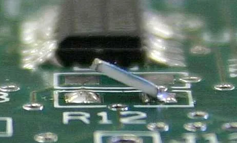
Several types of SMT defects can occur during the assembly process. Tombstoning, where a component stands upright due to uneven soldering, often results from improper pad design or reflow profiles. Bridging, another defect, happens when solder connects adjacent pads, typically due to excessive solder paste or incorrect stencil alignment. Component misalignment may stem from pick-and-place machine errors or substrate warpage. These issues compromise component integrity and can lead to short circuits or open connections. Electrical defects, such as insufficient contact, might arise from poor solder wetting or contamination on the board surface. Identifying the root causes of these SMT defects through systematic testing is crucial for maintaining assembly quality.
Key Testing Methods in SMT Assembly
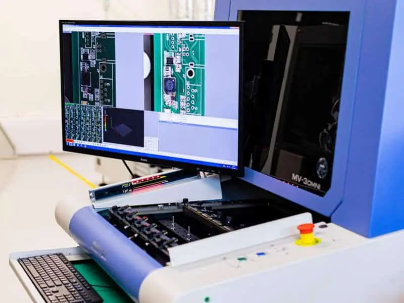
Several testing methods are employed to ensure the quality of SMT assemblies. Automated Optical Inspection (AOI) uses cameras to detect visual defects like misalignment or missing components. X-ray inspection is utilized for non-visible issues, such as voids in solder joints under components like Ball Grid Arrays (BGAs). In-Circuit Testing (ICT) evaluates electrical performance by checking for shorts, opens, and component values through test probes. Functional testing simulates real-world operating conditions to confirm overall board performance. Each method targets specific aspects of SMT testing, ensuring comprehensive defect detection. Standards like IPC-TM-650 provide guidelines for test procedures, ensuring consistency across different assembly environments. Engineers must choose the appropriate method based on the board’s complexity and application requirements.
Related Reading: Top 7 PCB Testing Methods to Guarantee Quality and Reliability
A Step-by-Step Breakdown of the SMT Testing Process
The SMT testing process is integrated into the full assembly workflow to catch SMT defects at the earliest possible stage. Below is a detailed breakdown of the four key phases, including typical defects encountered and the primary detection methods used.
The Pre-Reflow SMT Testing Process: Solder Paste Inspection (SPI)
Before components are placed, SPI systems use 3D laser or structured-light scanning to measure paste volume, height, and alignment on every pad. Common defects include insufficient solder (leading to open circuits), excess paste (causing bridges), and misalignment. SPI detects these with ±5 μm accuracy, catching up to 90% of printing-related issues before they reach reflow. Early correction prevents downstream rework and improves first-pass yield.
Mid-Stream SMT Testing: Post-Placement Inspection
After automated placement but before reflow, AOI or high-resolution cameras scan for component presence, polarity, and offset. Typical defects here are misalignment (±0.1 mm or greater), missing or damaged parts, and tombstoning precursors from paste issues. Vision systems flag errors in real time, allowing immediate rework or machine recalibration. This stage reduces placement-related SMT defects by 70–80% before soldering locks them in.
Post-Reflow SMT Testing Process: Ensuring Solder Joint Integrity
Immediately after reflow, AOI combined with X-ray inspection verifies joint quality. Common defects include tombstoning/Manhattan effect, solder bridges, voids, poor wetting, lifted leads, and solder balls. AOI handles visible issues while X-ray reveals hidden voids or cracks under BGAs and QFNs. This phase confirms mechanical and thermal integrity, catching 95% of reflow-induced SMT defects before final electrical testing.
Final Validation in SMT Testing: ICT and Functional Testing
At the end of the SMT testing process, ICT uses flying probes or bed-of-nails to verify shorts, opens, and component values. Functional testing then runs the board under simulated operating conditions to validate overall performance. Remaining defects (e.g., intermittent connections or functional failures) are detected here. ICT provides rapid electrical verification, while functional testing confirms real-world behavior, ensuring zero-defect shipment.
Related Reading: Common SMT PCB Assembly Defects
Comparing Key Methods within the SMT Testing Process
| Testing Method | Workflow Stage | Advantages | Disadvantages | Relative Cost | Best For |
|---|---|---|---|---|---|
| SPI (Solder Paste Inspection) | Pre-Reflow | Detects volume/alignment issues early; 3D accuracy | Limited to paste only | Low–Medium | High-volume printing lines |
| AOI (Automated Optical Inspection) | Post-Placement & Post-Reflow | Fast, non-contact visual defects; AI-assisted | Cannot see under components | Medium | Visible misalignment & bridges |
| X-ray Inspection | Post-Reflow | Reveals hidden voids, cracks, BGA issues | Slower, higher equipment cost | High | BGAs, QFNs, dense boards |
| ICT (In-Circuit Testing) | Final Validation | Electrical verification (shorts/opens/values) | Requires fixtures or probes | Medium–High | Electrical connectivity |
| Functional Testing | Final Validation | Simulates real-world operation | Longest test time; board-specific | High | Overall system performance |
Importance of Industry Standards in SMT Testing Process
Adherence to industry standards is non-negotiable for reliable SMT testing. Standards such as IPC-A-610H provide detailed criteria for acceptable solder joints and component placement. IPC-TM-650 offers test methods for evaluating board materials and assembly processes. Following these guidelines ensures consistency in detecting SMT defects and verifying component integrity. Additionally, standards like JEDEC J-STD-020E classify moisture sensitivity levels for components, aiding in proper handling during testing. Compliance not only enhances product quality but also builds trust in the assembly process. Engineers must stay updated on revisions to these standards to align SMT testing practices with the latest industry expectations.
Troubleshooting Insights for SMT Testing Challenges
In real-world scenarios, SMT testing can present unique challenges. One common issue is false positives during AOI, where acceptable variations are flagged as defects. This can be resolved by fine-tuning inspection parameters or cross-verifying with manual inspection. Another challenge is testing high-density boards with limited test point access. In such cases, combining ICT with functional testing can provide a more comprehensive assessment. For BGAs, X-ray inspection is indispensable to detect hidden solder voids, but interpreting results requires expertise. Engineers should also watch for environmental factors like humidity, which can affect test accuracy. Following guidelines from IPC-TM-650 for environmental testing conditions helps mitigate such issues. These troubleshooting strategies ensure that SMT testing remains effective even in complex scenarios.
Conclusion
The SMT testing process is a cornerstone of reliable electronics manufacturing, catching SMT defects at every critical stage—from paste printing through final validation. By integrating SPI, AOI, X-ray, ICT, and functional testing, engineers can ensure solder joint integrity, component alignment, and overall board performance. Adhering to standards like IPC-A-610H while applying proactive DFM and real-time inspection dramatically reduces rework and field failures. As devices grow more complex, a well-structured SMT testing process remains the key to delivering high-quality, defect-free assemblies that power modern technology.
FAQs
Q1: What are the most common SMT defects identified during PCB testing?
A1: Common SMT defects include tombstoning, solder bridging, and component misalignment. These issues can arise from uneven soldering, excessive paste, or equipment errors. Early detection through SMT testing methods like AOI or X-ray is crucial for maintaining quality.
Q2: How does SMT testing ensure component integrity in assemblies?
A2: SMT testing verifies component integrity by checking physical placement and electrical performance. Methods like In-Circuit Testing confirm connections, while functional testing simulates real-world conditions. This approach ensures reliable operation in the final product.
Q3: Which SMT testing method is best for detecting hidden defects?
A3: X-ray inspection excels at revealing hidden SMT defects such as solder voids under BGAs. Guided by IPC-TM-650, it provides accurate internal analysis when combined with other tests.
Q4: Why are industry standards important for SMT testing processes?
A4: Standards like IPC-A-610H define acceptance criteria and best practices across the SMT testing process. Compliance ensures consistent results, minimizes SMT defects, and meets high-reliability requirements.
References
- IPC-A-610H — Acceptability of Electronic Assemblies. IPC, 2021.
- IPC-TM-650 — Test Methods Manual. IPC, Current Version.
- IPC-7711/7721C — Rework, Modification and Repair of Electronic Assemblies. IPC, 2021.
- JEDEC J-STD-020E — Moisture/Reflow Sensitivity Classification for Nonhermetic Surface Mount Devices. JEDEC, 2014.


