Vias are unavoidable in PCB design, but they are not electrically transparent. Every via introduces parasitic capacitance and inductance that can degrade signal integrity, especially on high-speed nets. Understanding how to select via dimensions and manage their parasitic effects helps strike the right balance between routing flexibility, manufacturability, cost, and signal quality.
Selecting Via Types and Sizes
Common through-hole via options (in mil) include these drill/pad combinations:
- 8/16 ± 2 mil
- 10/20 ± 2 mil
- 12/24 ± 2 mil
As a practical guideline, when component density is high and routing space is scarce, smaller vias such as 8/16 (variations like 8/14, 8/16, 8/18) are often used. When placement is sparse and space allows, larger vias such as 12/24 (e.g., 12/22, 12/24, 12/26) are acceptable. For designs that fall in between, 10/20 (e.g., 10/18, 10/20, 10/22) is a common choice.
From a cost perspective, larger vias are generally cheaper to fabricate because they are less demanding on drilling and plating processes. If cost control is important and the design allows it, use larger vias while still meeting the electrical and density requirements.
In the HDI PCB design, blind and buried vias are often required. A common blind-via size is around 4/10 ± 2 mil. These blind vias are typically placed on pads; however, avoid drilling at the exact center of the pad. Shifting the via toward the pad edge can simplify processing for some manufacturing flows.

Manufacturing Constraints: Drill-to-Thickness Ratio
Via diameter cannot be arbitrarily reduced. A practical constraint is that the via’s finished hole diameter should not be smaller than approximately one-seventh of the PCB thickness. When the drill diameter falls below this ratio, plating distribution in the hole becomes difficult to control. Non-uniform copper plating on the via wall can compromise both reliability and electrical performance. For thicker boards, increase the via diameter accordingly.
Parasitic Capacitance and Inductance of Vias
Although vias are short structures, at high data rates they behave as discontinuities with parasitics that alter impedance, cause reflections, and distort waveforms. Two simple models—parasitic capacitance and parasitic inductance—are useful to understand the trends and the levers designers can pull.
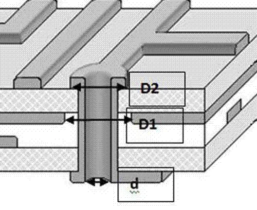
Figure 1 | Via parasitic capacitance model.
Via Parasitic Capacitance
A commonly used approximation for via capacitance is:
C = 1.41 ε T D2 / (D1 ? D2)
where:
- ε is the dielectric constant (relative permittivity) of the PCB material, which varies by laminate.
- T is the board thickness.
- D2 is the via’s outer diameter (often the pad diameter in the plane layer context).
- D1 is the clearance (anti-pad) diameter on a plane layer (distance from via edge to copper in the plane opening).
From this relationship:
- With board material and thickness fixed, increasing the anti-pad diameter D1 reduces via capacitance (C is inversely related to D1).
- With material and thickness fixed, increasing D2 increases via capacitance (C is directly related to D2).
- With D1, D2, and thickness fixed, higher dielectric constant increases via capacitance (C scales with ε).
- With ε, D1, and D2 fixed, increasing board thickness T increases via capacitance.
Via Parasitic Inductance
The via inductance can be approximated by:
L = 5.08 h [ln(4h/d) + 1]
where:
- h is the via length, approximately the board thickness for a through via.
- d is the via’s finished hole diameter (inner diameter).
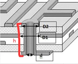
Figure 2 | Via parasitic inductance model.
From this relationship:
- Thinner boards reduce via inductance (L increases with h).
- Larger hole diameters reduce via inductance (L decreases as d increases).
Figure 3 | Inductance increases with via length and decreases with larger hole diameter.
Design Implications and Practical Guidelines
On low-speed or purely DC nets, via parasitics are usually negligible and standard via choices are sufficient. In high-speed designs, however, the capacitance and inductance of vias combine with trace and plane discontinuities to alter impedance and create reflections, slowing down edges and degrading eye margins. To mitigate these effects:
- Select reasonable via dimensions. For multilayer boards of typical density, a 10/20/36 mil configuration (drill/pad/anti-pad in plane) is often a good baseline. For power and ground connections, consider larger vias to lower impedance.
- Use a larger anti-pad (clearance) where feasible, especially in power or ground planes. A larger anti-pad reduces via-plane capacitance.
- Minimize layer transitions on high-speed signals. Fewer vias mean fewer discontinuities and less accumulated parasitic loading.
- Use thinner boards when practical to lower both via capacitance (via-to-plane spacing changes) and via inductance (shorter via length h).
Cost, Density, and Process Trade-offs
Design choices require balancing routing density, performance, and manufacturing cost. Smaller vias free up routing channels and reduce via capacitance, which is beneficial for high-speed signals. However, reducing via size increases fabrication cost and complexity and is limited by drilling and plating capability. In high-density designs, blind and buried vias can improve routing efficiency, but they also raise cost. Via dimensions cannot be reduced indefinitely; they are constrained by drill aspect ratio, plating uniformity, and yield. A balanced approach is essential.
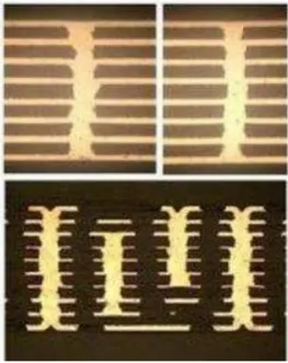
Why Limit the Number of Vias on a High-Speed Trace?
Each via adds an impedance discontinuity, parasitic capacitance, and inductance. These effects accumulate with every layer transition along a signal path. As the number of vias increases, reflections and edge degradation worsen, and eye opening and timing margins shrink. For this reason, many device and interface guidelines specify limits on the number of vias allowed on high-speed traces. A common rule of thumb is to keep the via count to three or fewer on sensitive high-speed nets—and to avoid vias altogether when possible.
In summary, treat vias as part of the transmission path. Choose dimensions that meet both process and electrical needs, allocate sufficient anti-pad clearance, minimize layer transitions, and avoid overshrinking via sizes beyond what the process can reliably support. This disciplined approach will reduce discontinuities, improve signal integrity, and increase the likelihood of first-pass success in high-speed PCB designs.