USB, short for Universal Serial Bus, is a serial-bus standard and I/O interface specification widely used in personal computers, mobile devices, and consumer electronics such as cameras, set-top boxes, and game consoles. USB 2.0 supports data rates up to 480 Mbps. USB 3.0 increases the maximum signaling to 5 Gbps and introduces full-duplex data transfer. As data rates rise, PCB layout and routing for USB links must follow high-speed design practices to preserve signal integrity and ensure robust compliance and interoperability.
Figure 1 shows the pin assignments for USB 2.0 and USB 3.0 connectors.
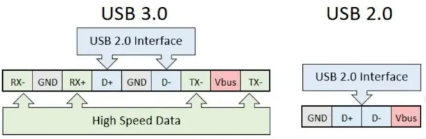
Figure 1 | USB 2.0 and USB 3.0 pin definitions
PCB Layout Requirements for USB Interfaces
Connector placement and mechanical considerations
- Place the USB receptacle at the board edge or as constrained by the product enclosure so the mating interface is accessible. For right-angle receptacles, allow the shell to properly overhang the PCB edge to meet the connector's mechanical requirements and to facilitate smooth insertion and removal.
- Arrange protection and filtering devices close to the connector in the following order along the signal path: ESD protection → common-mode choke → any RC components. This order clamps ESD strikes at the entry point and suppresses common-mode noise before it can couple into the rest of the system.
- Maintain a small but adequate gap between the connector and the ESD array to accommodate assembly tolerances and rework while keeping stub length minimal. Keep the placement symmetrical between the two lines of each differential pair.
- Plan component placement so the differential traces (D+/D- for USB 2.0, and the RX/TX differential pairs for USB 3.x) are as short and as direct as possible.
PCB Routing Requirements for USB Interfaces
Differential impedance, length, and shielding
- Route as differential pairs with controlled impedance of 90 Ω differential. Use consistent pair spacing and width to maintain coupling and minimize differential-to-common-mode conversion. Where possible, provide ground reference adjacent to the pair and, if used, guard ground on the sides to reduce crosstalk. Keep the total length short; for typical designs, keeping the length within about 1800 mil helps reduce insertion loss and jitter.
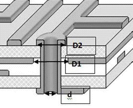
- Minimize layer transitions and vias on the high-speed USB differential pairs. Each via introduces impedance discontinuity and additional inductance/capacitance that can cause reflections. Keeping the pairs on one layer simplifies impedance control and lowers loss.
- When a layer change is unavoidable, place a pair of stitching ground vias close to the differential vias to provide a continuous, low-inductance return path. This helps the return current transition between reference planes and reduces loop area and mode conversion.
- If the connector's mounting posts or shell connect to protective/chassis ground, isolate this protective ground region from the signal ground by a 2 mm gap. Within the protective ground region, use a dense via pattern to lower inductance and create a robust path for ESD and EMI currents to return to the chassis.
Length matching and skew control
- Unequal lengths in a differential pair produce intra-pair skew. Skew converts part of the differential signal into common-mode energy, increases susceptibility to EMI, and degrades the eye opening. Compensate for unavoidable differences by length-tuning the shorter line. Keep the intra-pair length difference within 5 mil, and follow good differential tuning practices so the added serpentine does not create tightly coupled meanders that increase local crosstalk.
Example layouts
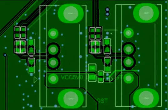
Figure 2 | USB 2.0 layout and routing
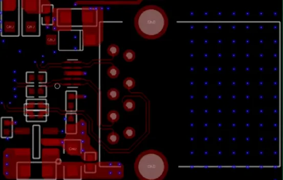
Figure 3 | USB 3.0 layout and routing
PCB Design for USB Type-C Interfaces
USB Type-C, commonly referred to as USB-C, is a reversible connector specification independent of the USB protocol version. Its key advantages include a much thinner mechanical profile, support for higher data rates (up to 10 Gbps under appropriate protocols), and enhanced power delivery (up to 100 W depending on the negotiated power profile). The reversible plug supports insertion in both orientations, enabling compact designs. Figure 4 shows the USB Type-C receptacle pinout.
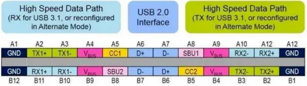
Figure 4 | USB Type-C receptacle pin assignments
Protection and filtering order
- Place ESD protection and common-mode chokes as close to the Type-C connector as possible in the order: ESD → common-mode choke → any RC elements. Maintain a small clearance between the connector shell and the ESD array to balance assembly robustness and electrical performance.
AC coupling capacitors for SuperSpeed pairs
- Place the AC-coupling capacitors for the TX differential pairs near the connector. The RX side AC-coupling capacitors are provided on the device end. Figure 5 illustrates the typical placement for TX AC-coupling capacitors. Locating these capacitors near the connector helps minimize stubs and preserves launch symmetry, both of which improve return loss at the channel entry.
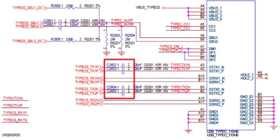
Figure 5 | TX AC-coupling capacitor placement
Impedance control and reference planes
- Route Type-C differential pairs with 90 Ω ± 10% differential impedance. Use continuous reference planes and do not cross plane splits. Limit layer transitions; when a layer change is necessary, keep the number of signal vias per differential pair to two or fewer. Adjacent ground stitching vias at each transition preserve the return path and reduce mode conversion. Maintaining impedance and reference continuity minimizes reflections that would otherwise degrade insertion and return loss.
Pair count, stackup guidance, and path length
- Type-C exposes four SuperSpeed differential pairs (RX1/TX1 and RX2/TX2) and two USB 2.0 differential pairs (D+/D-), for a total of six differential pairs. Route these pairs with at least one adjacent ground plane; having ground reference on both sides of the signal layer further improves field containment. Keep the routes as short and direct as possible, and avoid total lengths exceeding 6 inches to limit insertion loss and timing uncertainty.
Length matching and spacing
- Match the lengths within each differential pair; keep intra-pair skew below 6 mil. Maintain consistent pair spacing and the intended coupling along the entire path. For isolation, keep spacing between separate differential pairs—and between a pair and unrelated signals—at least 4× the Type-C differential trace width when feasible. Greater spacing reduces near-end and far-end crosstalk and helps preserve eye opening at the receiver.
CC pins and power configuration
- The CC1/CC2 pins are critical for connection detection, plug orientation, host/device role determination (DFP/UFP), and VBUS configuration. Route CC lines with care and use wider traces as appropriate to meet current-handling and robustness needs, especially in designs that negotiate higher power levels.
High-speed connector breakout considerations
When signaling rates approach or exceed 8 Gbps, pay special attention to the connector launch and breakout region. Apply advanced high-speed connector optimization techniques to reduce reflections and resonances. Typical approaches include minimizing stub length in the breakout, optimizing pad and anti-pad geometries, keeping launches symmetrical across the pair, and tightly controlling the reference plane transitions. These measures help maintain a well-behaved channel through the most discontinuity-prone portion of the link.
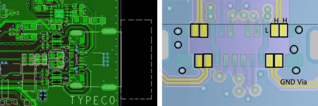
Figure 6 | Type-C connector routing illustration
Why these rules matter
The guidelines above reflect core high-speed signal-integrity principles. A USB differential link is a transmission line: any impedance discontinuity (from width changes, via transitions, or connector launches) reflects part of the incident wave back toward the source. Reflections, common-mode conversion, and crosstalk reduce the eye opening at the receiver and consume timing and voltage margins. Keeping pairs short, closely coupled, and referenced to solid ground planes lowers emitted and conducted noise. Proper ESD placement protects the system at the boundary without adding excessive capacitance mid-channel. Ground isolation between the connector shell and signal ground provides a low-impedance path for ESD and EMI currents to return to chassis while preventing DC ground loops in the logic domain. Careful length matching limits skew, so the receiver sees a clean, symmetric differential signal with minimal common-mode content. Together, these practices help USB 2.0 and USB 3.x links meet compliance while improving robustness in real-world systems.
By combining disciplined placement, controlled-impedance routing, robust return-path design, and targeted protection at the connector, engineers can achieve reliable USB performance across a wide range of products—from cost-optimized USB 2.0 implementations to compact, high-bandwidth designs with USB Type-C.