 00:55
00:55
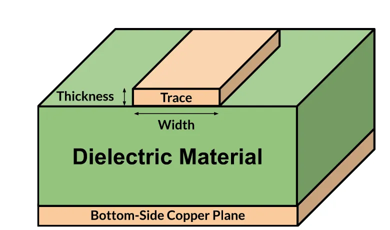
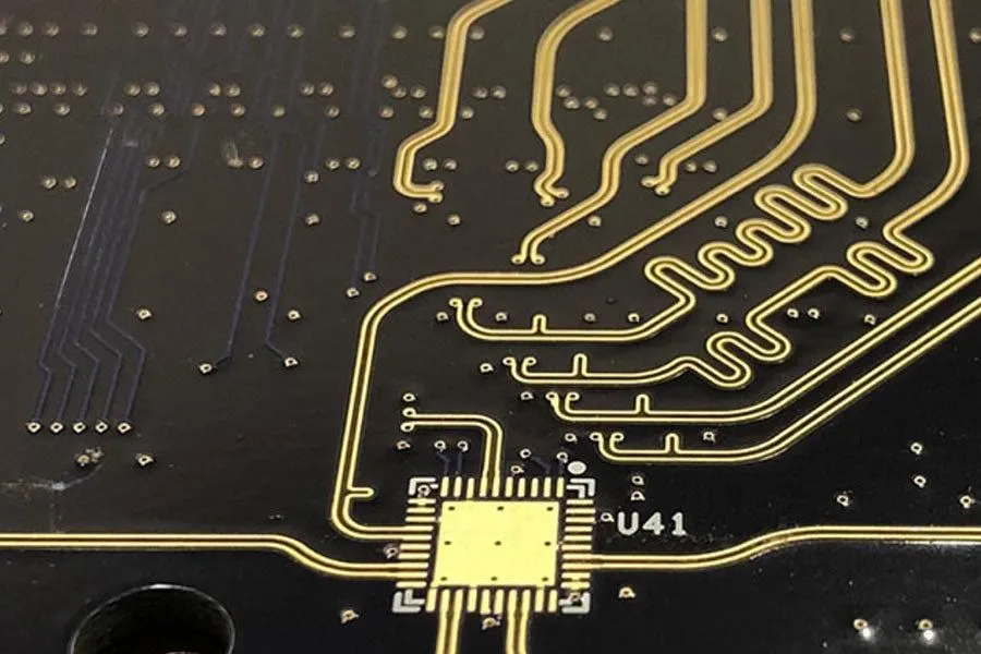
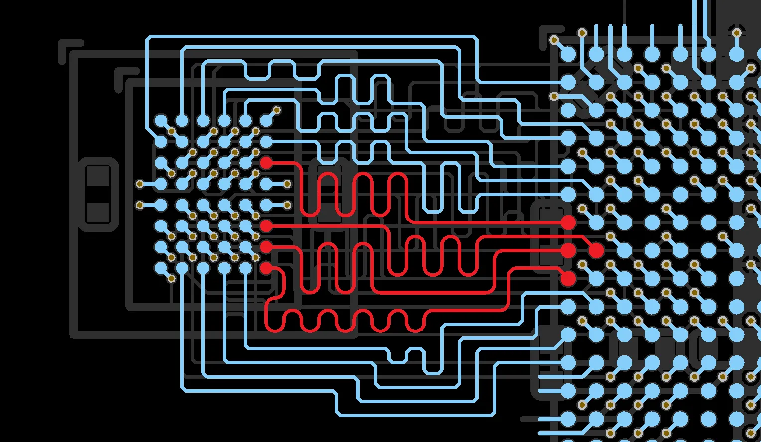
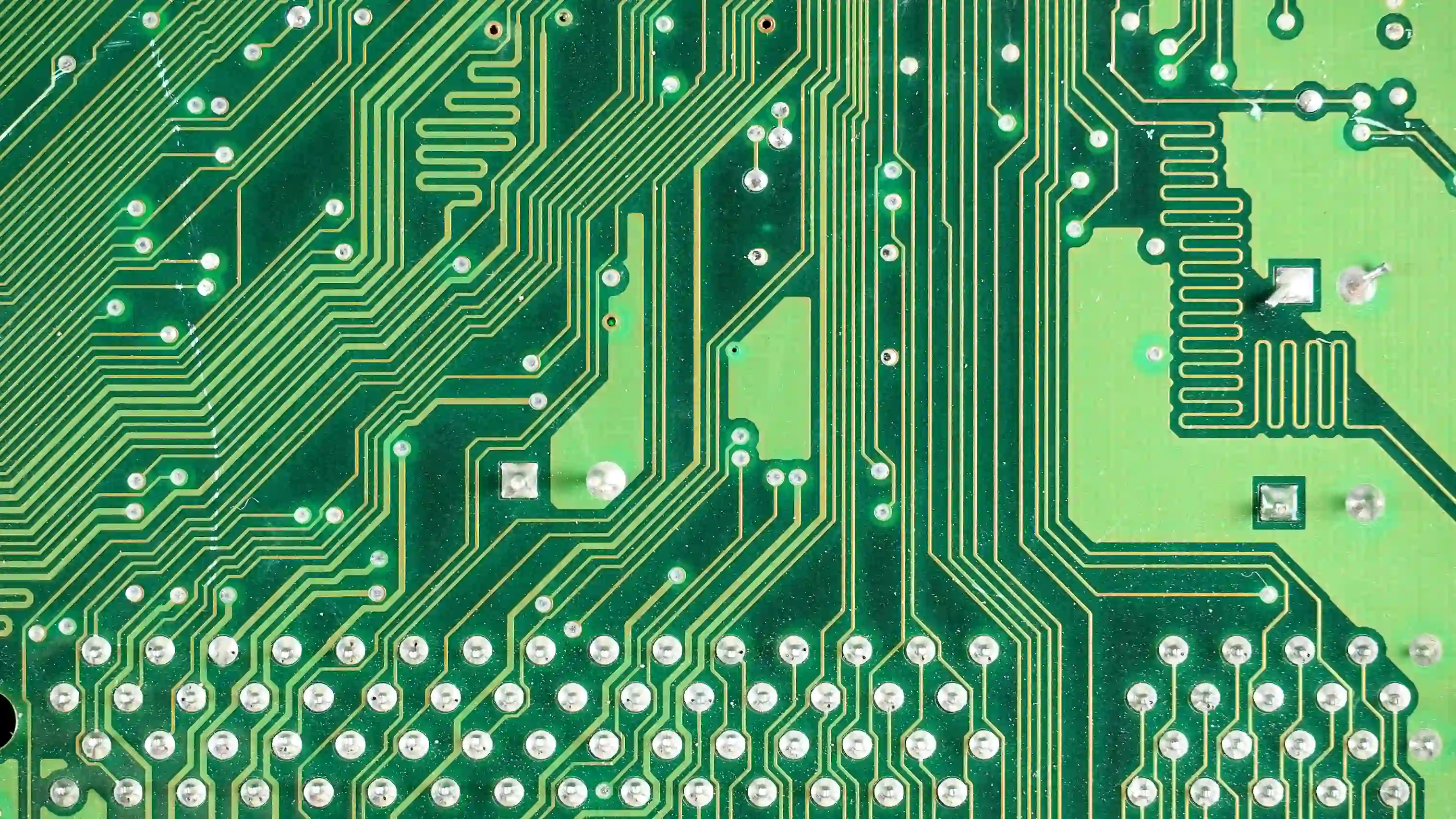
PCB Trace
PCB traces form the essential conductive pathways on a printed circuit board, enabling the flow of electrical signals between components. Understanding PCB trace design is crucial for engineers, hobbyists, and manufacturers aiming to optimize circuit performance, minimize signal interference, and ensure reliability in electronic devices. This tag, PCB Trace, encompasses a range of articles that delve into the fundamentals and advanced techniques for creating effective trace layouts, from basic routing principles to complex considerations like impedance matching and thermal management. For those searching for guidance on PCB traces, the content here addresses common challenges such as calculating trace width to handle specific current loads, preventing crosstalk in high-speed designs, and adhering to industry standards like IPC-2221 for durability. Practical applications include tips for multilayer boards where traces must navigate dense component arrangements without compromising signal integrity. Best practices highlighted in these articles emphasize using simulation tools to predict electromagnetic behavior, selecting appropriate copper thicknesses, and implementing ground planes to reduce noise—insights that can directly improve your prototyping and production processes. Whether you are troubleshooting trace-related issues in an existing design or starting a new project, the articles under this tag offer step-by-step advice and real-world examples. Exploring them can help you refine your skills, avoid costly errors, and achieve more efficient PCB layouts tailored to applications in consumer electronics, automotive systems, or IoT devices.
Video Guide
-
00:55
Technical Articles
Essential Guide to Trace-to-Pad Clearance in PCB Design
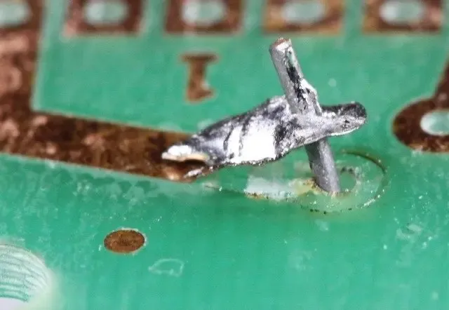
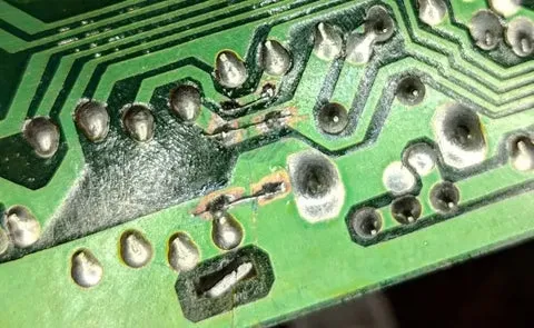
Lifted Pads: Diagnosing PCB Damage and Implementing Effective Repair Strategies
Trace Shorts: How to Find and Fix Them Quickly!
PCB Trace Width and Footprint Compatibility
DIY Trace Repair: Saving Your Project from a Broken PCB
How to Avoid Common PCB Design Mistakes with 1 oz Copper
PCB Assembly Cost
RF PCB Design for Beginners: A Complete Introductory Guide
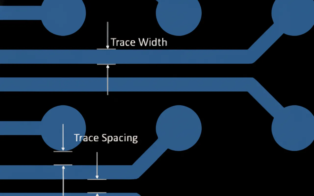
What are PCB Traces?
How Does PCB Trace Width Affect Impedance?
How to Calculate PCB Trace Width for 20A Circuits
Understanding Trace Width Tolerances in PCB Manufacturing for Reliable Designs
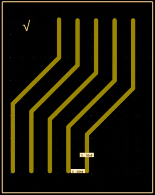
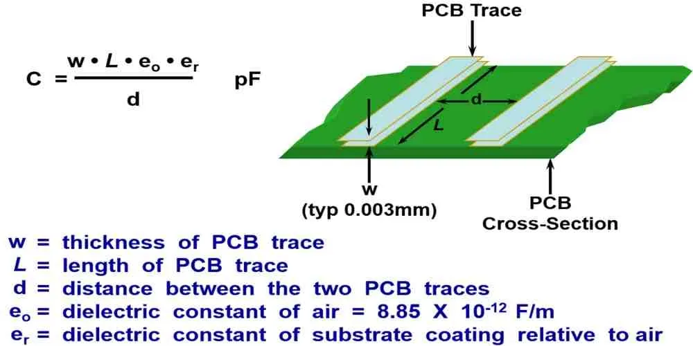
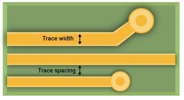
How to Calculate Optimal Trace Spacing in PCB Design
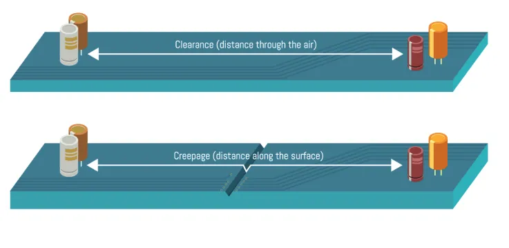
Optimizing PCB Trace Clearance: A Guide to Reliable Circuit Board Design
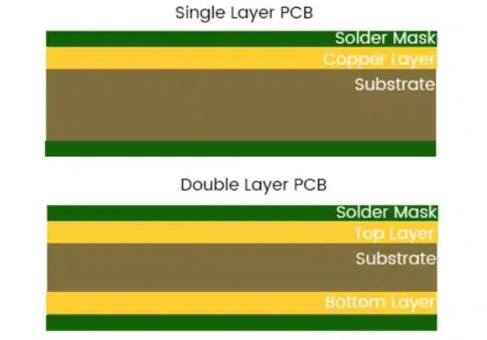
Understanding PCB Basics: Layers, Traces, and Vias Explained
The Impact of PCB Trace Width on Solar Inverter Efficiency: A Detailed Analysis
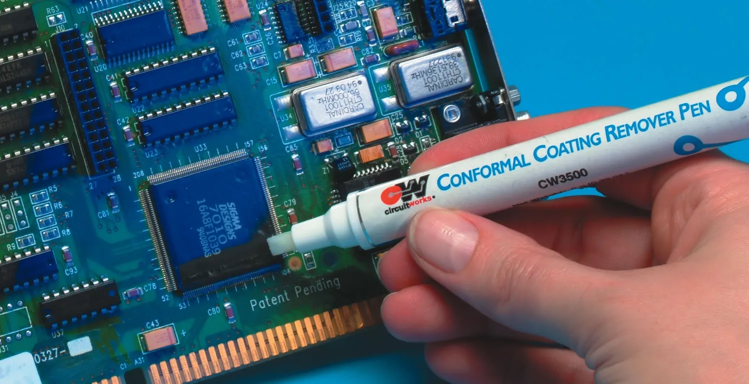
PCB Repair Techniques: Fixing Damaged Traces and Pads with Precision Tools
Get in Touch
Send Message
- Products & Service
- Company
- About AIVON
- Contact
- News
- Blog
- Certification
-


- Payment
-


2026 AIVON.COM All Rights Reserved