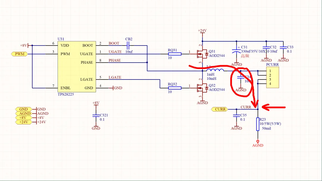
This article analyzes the output current waveform of a PWM current-control stage that uses an LC filter at the output. A PWM voltage is applied to an output network composed of inductor L1 and capacitor C34. After filtering, current flows through a 25 Ω load resistor and a shunt resistor R23 used for current sensing. The output capacitor C34 significantly affects the current waveform. By measuring the shunt voltage (proportional to output current) at different capacitor values and modeling the response, we extract parameters that support subsequent constant-current controller design.
Data Acquisition and Preprocessing
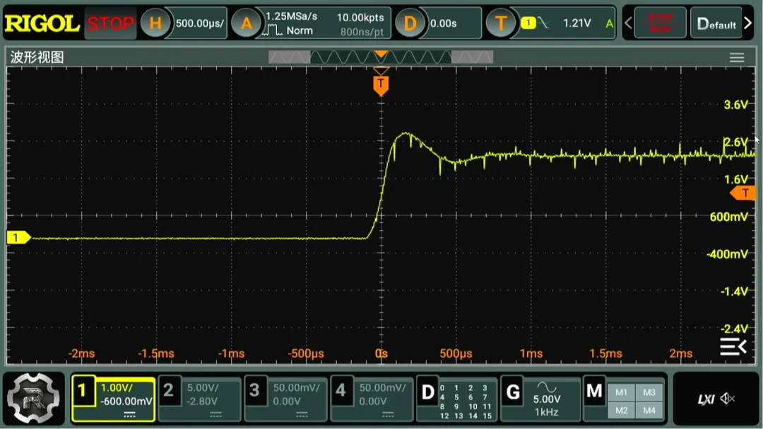
Measurements focus on the shunt resistor R23, whose voltage tracks the output current. For the case with an output capacitor of 10 μF, we captured the unit step response at the rising edge (10k samples at a 20 MHz sampling rate), and similarly captured the falling-edge response. For comparison, measurements with a 0.1 μF output capacitor show a monotonic current waveform without overshoot. The overshoot observed in the 10 μF case is attributable to LC oscillation in the output network.
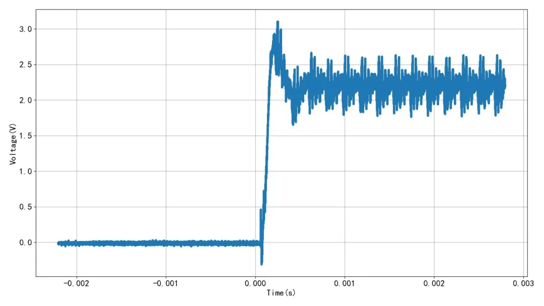
Figure 1 | Rising-edge current waveform (raw data)
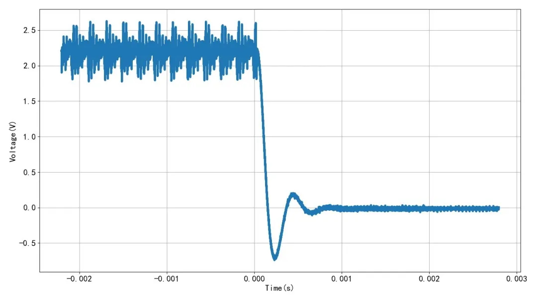
Figure 2 | Falling-edge current waveform (raw data)
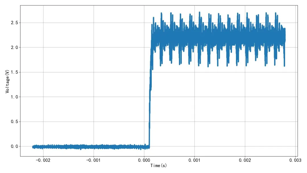
Figure 3 | Rising-edge waveform (additional capture)
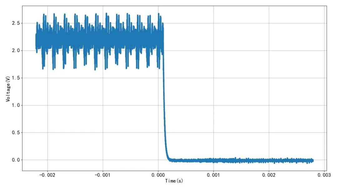
Figure 4 | Falling-edge waveform (additional capture)
The raw time-domain records contain substantial high-frequency interference. To isolate the dynamic behavior of the power stage relevant to control design, we applied a 4th-order Butterworth low-pass filter with a 200 kHz cutoff. This digital filtering effectively removes high-frequency noise while preserving the low- and mid-frequency dynamics that shape the step response. The filtered results provide a cleaner basis for parameter extraction and model validation.
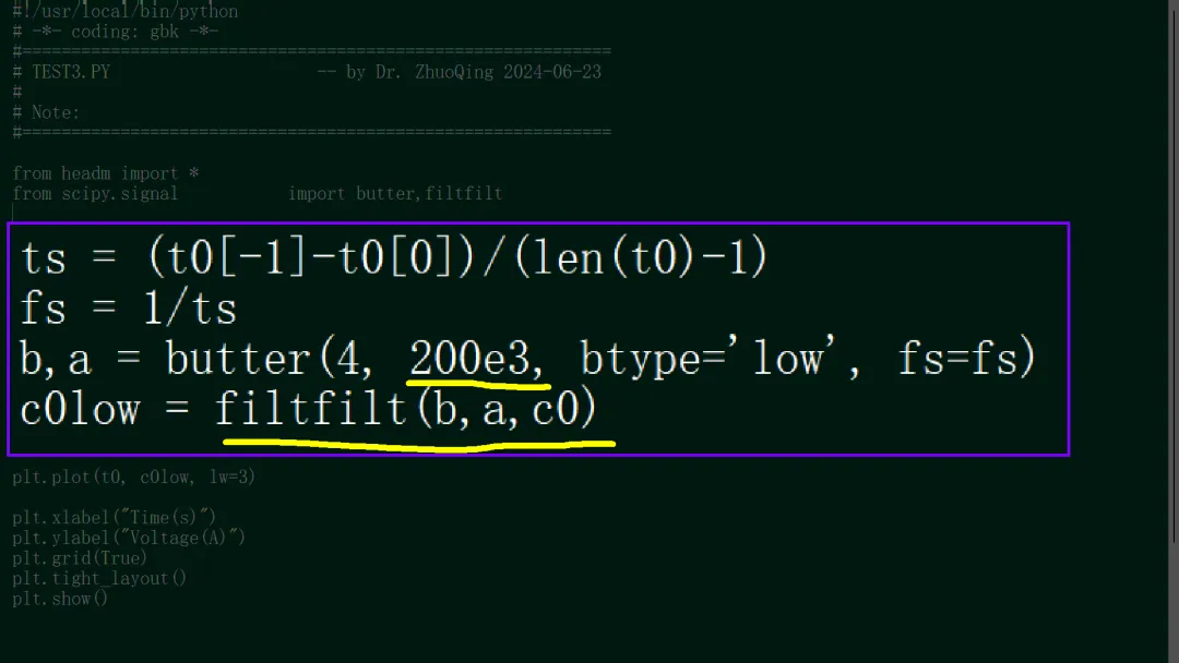
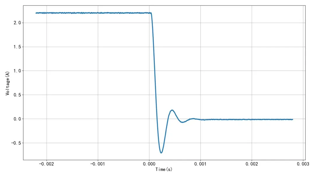
Figure 5 | Signal waveform after low-pass filtering
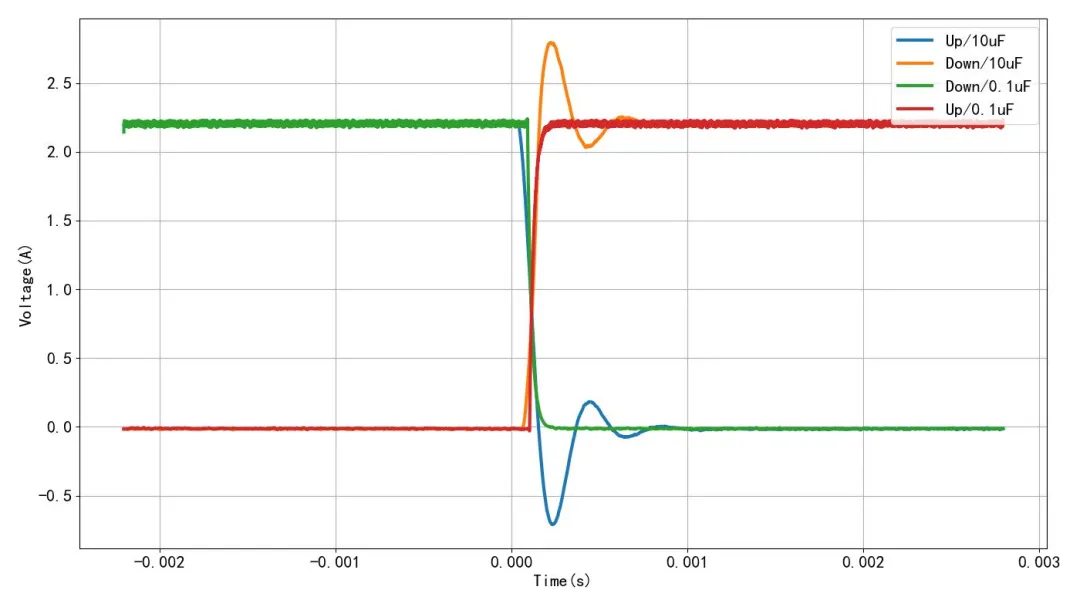
Figure 6 | Four waveforms after low-pass filtering
Step and Impulse Responses under Different Output Capacitors
The output stage dynamics are dominated by the LC filter and the load. With a 0.1 μF output capacitor, the measured unit step response of the current is well damped and exhibits no oscillation. In contrast, with a 10 μF output capacitor, the system becomes underdamped and the response exhibits overshoot and ringing, which aligns with expectations for an LC network with low loss.
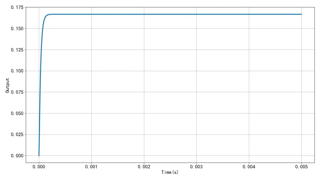
Figure 7 | Unit step response for C = 0.1 μF
A simplified linear model allows calculation of the unit impulse response for the 10 μF case. The computed impulse response shows an underdamped oscillation with a larger amplitude than observed in the measurements when ideal, lossless components are assumed. This discrepancy points to the damping provided by real-world parasitics, primarily series resistance.
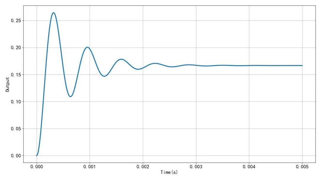
Figure 8 | Unit impulse response for C1 = 10 μF
Plant Modeling and Transfer Function
From the output network perspective, the LC filter together with the 25 Ω load establishes a second-order low-pass behavior. A simplified equivalent circuit can be drawn with L1 in series with the source, C34 shunting to ground at the output node, and the load resistor in parallel with the output. Using this equivalent, a transfer function can be established between the PWM drive (or its equivalent averaged voltage) and the measured output current (proportional to the shunt voltage). This transfer function forms the basis for analyzing step and impulse responses, and for designing a current-loop controller.
Two parameters govern the qualitative behavior of the response:
- The natural frequency of the LC network, which scales as 1/√(LC). Increasing C lowers the natural frequency, slowing the response and potentially increasing the quality factor Q.
- The damping, which is set by effective resistance in the system. This includes the load, the inductor's series resistance, capacitor ESR, and any intentional damping elements. Lower damping increases overshoot and ringing.
In the idealized lossless model, the predicted oscillation amplitude tends to be higher than what is measured on real hardware. Incorporating component parasitics, especially inductor series resistance, brings the model into closer agreement with measured behavior.
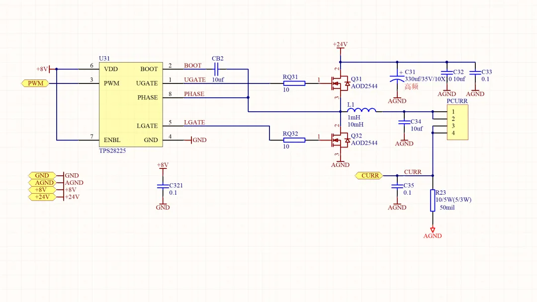
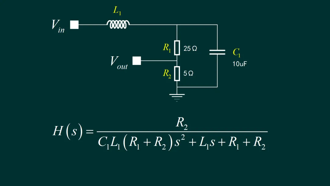
LTspice Simulation with Inductor ESR
To capture the damping observed on the bench, the inductor's equivalent series resistance (ESR) was included in the LTspice simulation model. The resulting waveforms closely match the measured current responses, validating that parasitic resistance is the dominant damping mechanism in this setup. This step is critical: without parasitics, the simulated response overestimates overshoot and ringing compared to actual hardware.
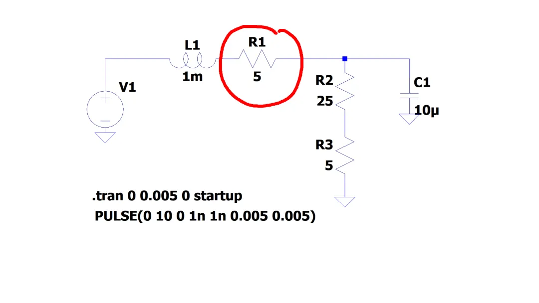
Transfer Function Including ESR and Step-Response Validation
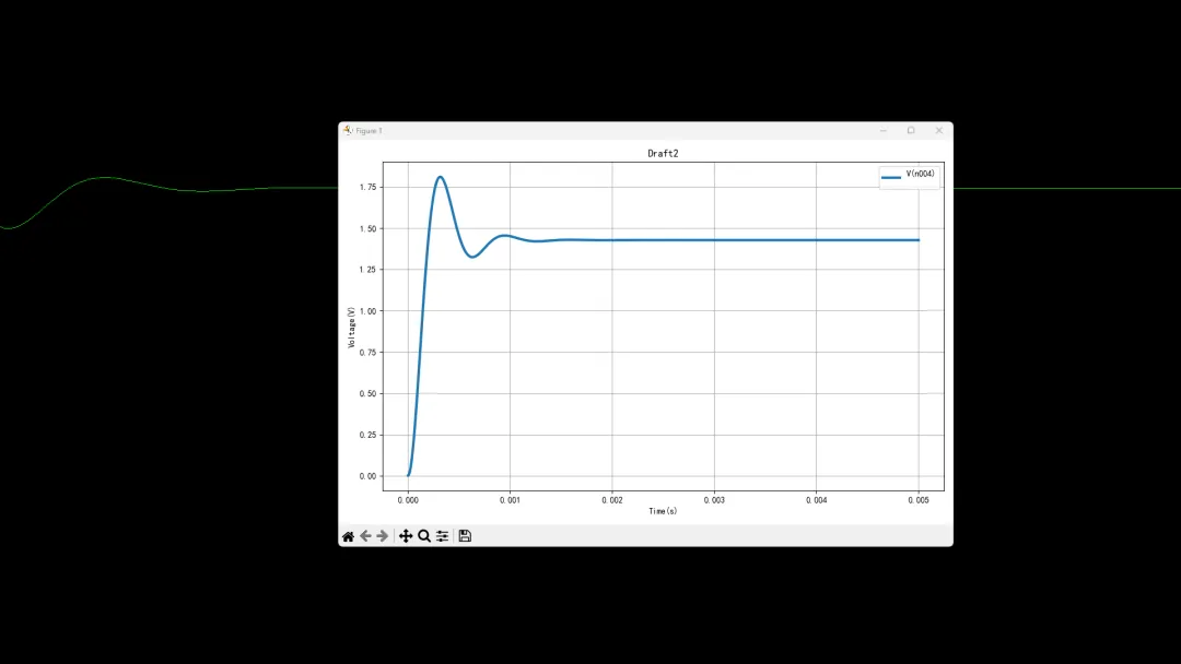
With inductor ESR accounted for, the transfer function of the output stage more accurately reflects the real plant. The unit step response derived from this transfer function aligns with the filtered measurement data, confirming the earlier conclusion: a larger output capacitor (10 μF) in a low-loss LC network yields an underdamped response with overshoot, whereas a much smaller output capacitor (0.1 μF) produces a monotonic response under the same load.
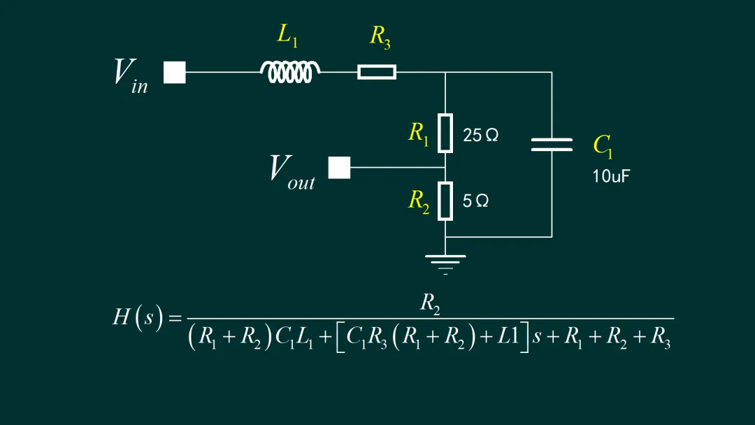
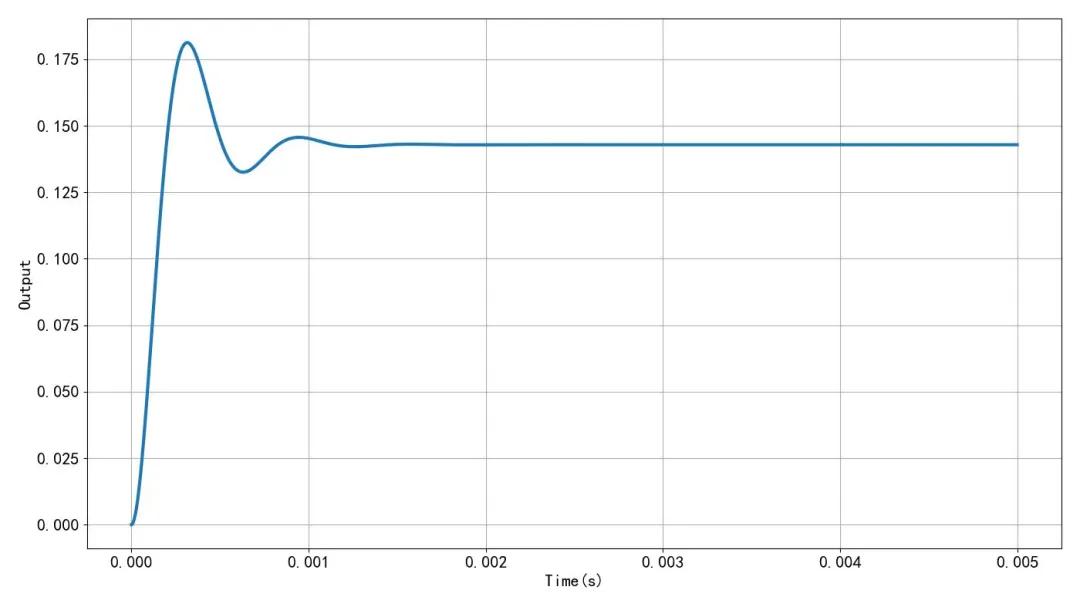
Figure 9 | Unit step response obtained from the transfer function (including inductor ESR)
Practical Implications for Constant-Current Control Design
The measurement and modeling workflow yields a plant model suitable for sizing and tuning a constant-current control loop. Several practical points follow from the results:
- PCB component selection sets the plant dynamics. Increasing C reduces the cutoff frequency but, in low-loss networks, also increases Q and the likelihood of overshoot. Conversely, smaller C values improve damping and response monotonicity but raise ripple and may amplify switching artifacts without adequate filtering.
- Realistic parasitic modeling is essential. Including inductor ESR (and, where relevant, capacitor ESR and wiring resistance) in simulations reduces the discrepancy between ideal predictions and bench measurements, enabling more reliable controller design.
- Digital preprocessing clarifies system dynamics. Applying a suitable low-pass filter (e.g., a 4th-order Butterworth at 200 kHz in this work) to the measured shunt waveform suppresses high-frequency switching noise and interference, revealing the underlying second-order dynamics needed for parameter extraction and control synthesis.
- Use both step and impulse perspectives. The unit step response captures time-domain characteristics such as rise time, overshoot, and settling, while the impulse response relates directly to the system's natural modes. Agreement between both, across measurement and model, increases confidence in the identified plant.
- Validate across operating transitions. Comparing rising and falling edges checks for asymmetries due to nonideal switching or component nonlinearities. Similar dynamics on both edges indicate the linear model adequately captures the dominant plant behavior for small-signal design.
With a validated plant model, controller bandwidth and compensation can be chosen to balance speed and robustness, ensuring sufficient phase margin even in the underdamped case. If a given capacitor value leads to unacceptable overshoot, adding damping (through component ESR, a small series resistor with the capacitor, or a snubber) can moderate the response without sacrificing low-frequency regulation.
Conclusion
The output current of a PWM current-controlled power stage was measured at the shunt under two output capacitor values (0.1 μF and 10 μF). After digital low-pass filtering (4th-order, 200 kHz), the data clearly reveal the LC-driven transient behavior. A simplified second-order plant model was developed, and its impulse and step responses were computed. Incorporating inductor ESR in LTspice produced simulations that closely match the filtered measurements: the 10 μF case exhibits underdamped overshoot due to low loss in the LC network, while the 0.1 μF case settles monotonically under the same 25 Ω load. These results provide a validated plant model and quantitative insight to guide the subsequent constant-current control design.