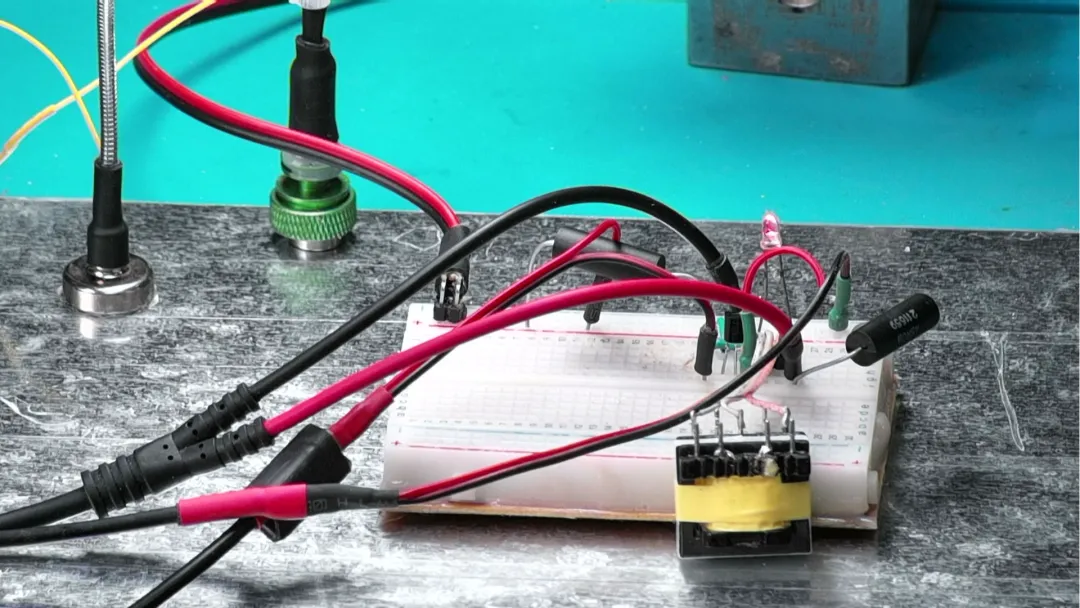
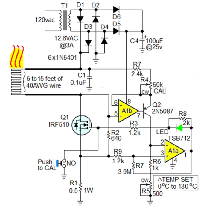
Infrared thermography provides non-destructive, non-contact temperature measurement and visualizes heat distribution and diffusion in real time. By converting surface infrared radiation into a thermal image, engineers can quickly assess where heat is generated, how it spreads, and which components or traces are operating outside their expected thermal range. As a result, thermal imaging has become a practical tool in PCB design verification, chip development, LED product R&D, and failure analysis.
Temperature is one of the dominant factors driving electronic reliability. Industry surveys report that approximately 55% of electronic device failures are temperature-related. As temperature rises, failure rates often increase exponentially because higher temperatures accelerate thermally activated wear-out mechanisms. Around the 70–80 °C operating range, a 1 °C increase can reduce component reliability by about 5%. For hardware teams, finding thermal hotspots early—during bring-up, validation, or environmental stress testing—can prevent field failures and design re-spins.
From Point Measurements to Full-Field Thermal Mapping
Traditional contact thermometry has clear limitations in electronics. Consider a motor controller R&D team tasked with locating potential overheating risks on a PCB and pinpointing the heat source quickly and accurately. With contact temperature probes, engineers might place 10 or more measurement points and wait for readings to stabilize. This process can take 30 minutes or more, and misplacement or probe slippage can force a restart. Small components are difficult to measure precisely, and point measurements miss the bigger picture—engineers are forced to analyze point by point rather than seeing the entire board’s thermal behavior at once.
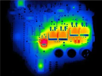
Infrared thermography solves these challenges. A single thermal image shows the board’s complete thermal field, allowing teams to immediately identify anomalous hotspots, verify heat-spreading paths, and compare temperature gradients across components, planes, and heat sinks. This full-field view accelerates root-cause isolation: engineers can see if a regulator is saturating, a MOSFET is operating with excessive switching loss, a linear regulator is undersized, or a copper pour is insufficient for a given current density.
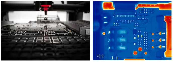
Figure 1 | Real-time thermal distribution visualization supports rapid identification of PCB fault locations.
Measuring Micro-Scale Targets: Macro Lenses and Thermal Sensitivity
Measuring micro-scale targets is a common challenge in electronics thermal testing. Contact sensors are constrained by probe size and cannot measure targets smaller than roughly 1 mm without significant error. High-end infrared cameras equipped with dedicated macro optics overcome this limitation by increasing optical magnification and reducing the instantaneous field of view (IFOV). With the right macro lens, micro-scale targets as small as 25 μm can be measured effectively, enabling temperature mapping across dense chip structures, fine-pitch packages, or narrow PCB traces.
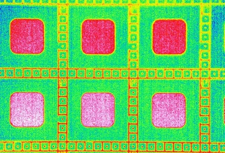
Thermal sensitivity, commonly specified as the noise-equivalent temperature difference (NETD), determines the smallest temperature change the camera can resolve. Systems with thermal sensitivity better than 25 mK can capture very subtle temperature variations and gradients. In lab measurements of lattice-like component arrays, for example, two adjacent rows might show 34.1 °C versus 34.2 °C, revealing small but meaningful differences in heat dissipation due to placement, airflow, copper distribution, or component tolerances. Such sensitivity allows R&D teams to compare layout options, verify the effectiveness of thermal vias, or identify marginal devices before they become failures.
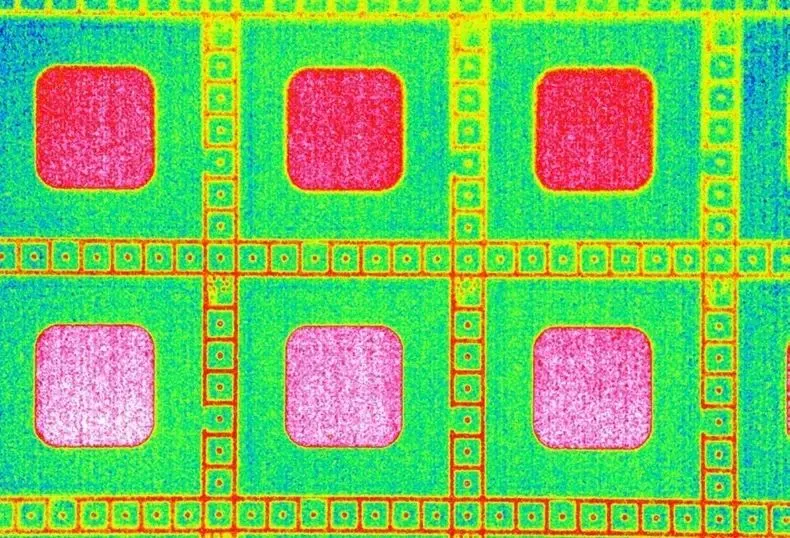
Figure 2 | Thermal imager fitted with a 25 μm macro lens for micro-target thermal analysis.
Online (fixed-mount) thermal imagers combined with macro lenses are also effective for continuous or automated testing. They can monitor micro-scale targets repeatedly under different input conditions, ambient temperatures, or airflow settings to build a comprehensive understanding of thermal behavior over time—useful for qualification and design-of-experiments workflows.
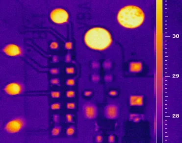
Figure 3 | With a macro lens, even fine PCB routing and small components can be clearly resolved in thermal images.
Selecting Optics for Electronics Thermal Testing
Choosing the right lens is essential to match working distance, field of view, and spatial resolution to the target and test setup. Typical options include:
- Standard lens: Suitable for most general-purpose electronics and electromechanical product testing where an overall thermal map is needed.
- Telephoto lens: Useful for distant targets, such as high-voltage equipment at distances beyond tens of meters, or when access is restricted.
- Wide-angle lens: Ideal for close-range, wide-area scenes—such as mapping the temperature distribution of a large HDI PCB inside an environmental chamber—when space is limited.
- Macro lens: Designed for micro-scale targets at close working distances (on the order of 100 μm features and smaller), enabling precise inspection of chip-level structures and fine traces.
When selecting optics, consider the minimum resolvable spot size relative to the smallest feature of interest. A general guideline is to ensure that the feature spans several pixels to obtain stable, accurate readings. Macro lenses increase the effective pixel density on the target and reduce parallax or averaging errors across adjacent hot and cool features.
Practical Workflow and Best Practices
To extract accurate, repeatable measurements from thermal images, integrate the following practices into your workflow:
- Emissivity and surface preparation: Many electronics surfaces—such as bare copper, tin, gold finishes, or polished metal heat sinks—are reflective and have low emissivity, which can cause apparent temperature errors due to reflections of surrounding objects. Set the emissivity in the camera to match the surface or apply a high-emissivity tape/paint dot at the measurement point to obtain a more reliable reading.
- Control reflections and background: Minimize reflections from hot tools, lamps, or nearby equipment. Shield the setup or use diffuse backgrounds to reduce spurious thermal contributions in the scene.
- Focus and IFOV: Achieve critical focus, especially with macro lenses where depth of field is shallow. Verify that the IFOV is smaller than the feature of interest and that the measurement spot is fully within the target area.
- Steady-state vs. transient capture: For steady-state evaluation, allow sufficient time for thermal equilibrium under typical load. For transients, use an appropriate frame rate and record video to capture inrush, startup, or load-step events with adequate temporal resolution.
- Reference markers and regions: Use point, line, and area tools to log temperatures across multiple components simultaneously. This speeds comparisons between different design iterations or operating conditions.
- Complementary measurements: Where absolute accuracy is critical, correlate thermal imaging with a calibrated contact sensor at a prepared high-emissivity spot to validate readings. Use electrical measurements (current, voltage, switching waveforms) to connect thermal symptoms back to circuit operation.
- Safety and access: For high-voltage or high-power systems, maintain appropriate clearance and isolation. One advantage of infrared cameras is safe, non-contact observation of live hardware that would be hazardous to probe directly.
Use Cases in Electronics and Semiconductor Work
Infrared thermography is broadly applicable across electronics R&D, production test, and failure analysis. Typical scenarios include:
- PCB evaluation: Identify overloaded regulators, MOSFETs with excessive conduction or switching losses, insufficient copper area, or poor thermal via placement. Validate heat sink performance and airflow patterns.
- Chip-level inspection: Map temperature on dies, packages, or bond wires to detect non-uniform heat generation, potential shorts, or defective units during device bring-up or reliability testing.
- LED devices: Measure junction-proximate temperatures and verify thermal coupling to substrates and heat spreaders to ensure lumen maintenance and lifetime targets.
- Display panels: Detect hot pixels and non-uniformities in LCDs or other displays, correlating thermal anomalies with functional defects.
- Environmental testing: Observe boards under thermal cycling or high ambient conditions to ensure margins remain adequate and that design fixes (e.g., heat spreaders, airflow ducting) are effective.
Interpreting Thermal Data to Improve Design
The value of thermal imaging comes from closing the loop between observation and design decisions. Examples include:
- Component placement and orientation: If similar parts exhibit different temperatures based on orientation or position—such as the 34.1 °C versus 34.2 °C difference observed between two rows—engineers can test alternative placements, flip packages to alter heat paths, or adjust spacing to reduce localized heating.
- Copper and via optimization: Thermal maps guide where to widen traces, add copper pours, or increase thermal via density to improve heat spreading from high-dissipation components.
- Power architecture and control: High temperatures may indicate a need to alter switching frequency, gate drive, or topology to reduce losses in power stages.
- Materials and interface quality: Elevated heat sink temperatures can signal poor thermal interface material coverage, insufficient clamping force, or surface flatness issues that increase interface resistance.
Infrared thermography turns temperature from a hidden variable into a visible, quantifiable design parameter. By rapidly locating fault points, validating thermal solutions, and enabling micro-scale inspection without physical contact, engineering teams can shorten debug cycles, reduce rework, and increase the reliability of shipped hardware.
Summary
For electronic systems where thermal performance directly affects reliability, infrared thermography provides fast, accurate, and comprehensive insight. Compared with point-by-point contact methods, it offers a full-field view that reveals hotspots immediately, supports precise micro-target measurements with macro lenses down to 25 μm, and resolves subtle temperature differences with high thermal sensitivity. Combined with sound measurement practices—emissivity control, proper optics, and correlation with electrical data—thermal imaging is a practical, high-impact tool from prototype through production test.
Lens Options at a Glance
Example configuration options for fixed-mount thermal imagers commonly used in electronics testing include:
- Standard lens: General-purpose temperature mapping for electronics and electromechanical assemblies.
- Telephoto lens: Long-distance inspection of high-voltage or inaccessible equipment.
- Wide-angle lens: Close-range, wide-area mapping such as inside environmental chambers.
- Macro lens: Micro-target inspection for features on the order of 100 μm and below.