 02:22
02:22
DFM For PCB
Design for Manufacturability (DFM) is a critical aspect of PCB development that ensures designs are optimized for efficient production, minimizing errors, costs, and time-to-market. In the realm of electronics engineering, DFM For PCB focuses on guidelines and strategies that bridge the gap between innovative circuit design and reliable manufacturing processes. Whether you are an experienced PCB designer troubleshooting production issues or a newcomer aiming to create prototypes without costly revisions, understanding DFM principles can significantly enhance your project's success rate. At its core, DFM For PCB involves evaluating design elements such as component placement, trace routing, layer stacking, and material selection to align with manufacturing capabilities. Common challenges like insufficient clearances, thermal management oversights, or incompatible fabrication tolerances often lead to defects during assembly. By incorporating DFM best practices early in the design phase, you can avoid these pitfalls, improve yield rates, and ensure compliance with industry standards like IPC-7351. For instance, adhering to rules for via placement and solder mask design not only reduces rework but also facilitates automated assembly lines, making it invaluable for high-volume production or complex multilayer boards. Our articles under this tag provide practical insights into implementing DFM techniques, from selecting appropriate board materials to conducting thorough design rule checks using tools like Altium or KiCad. You will find step-by-step guidance on optimizing layouts for wave soldering, reflow processes, and panelization, along with case studies demonstrating real-world applications in consumer electronics, automotive, and IoT devices. Delving into these resources equips you with the knowledge to refine your PCB designs, ultimately leading to more robust and economical outcomes in your engineering endeavors.
Video Guide


Technical Articles

Solder Mask "Dams" Between SMT Pads: A Complete Guide to Solder Mask Coverage and NSMD Design

Preventing Tombstoning and Cold Solder Joints in 0603-and-Smaller SMT Chips with Thermal Relief

SMT 0402/0201 Components: The 8 mil Pad Spacing Red Line

PTH Plated-Through-Hole Performance Metrics: The Hidden Lifeline of SMT Reliability
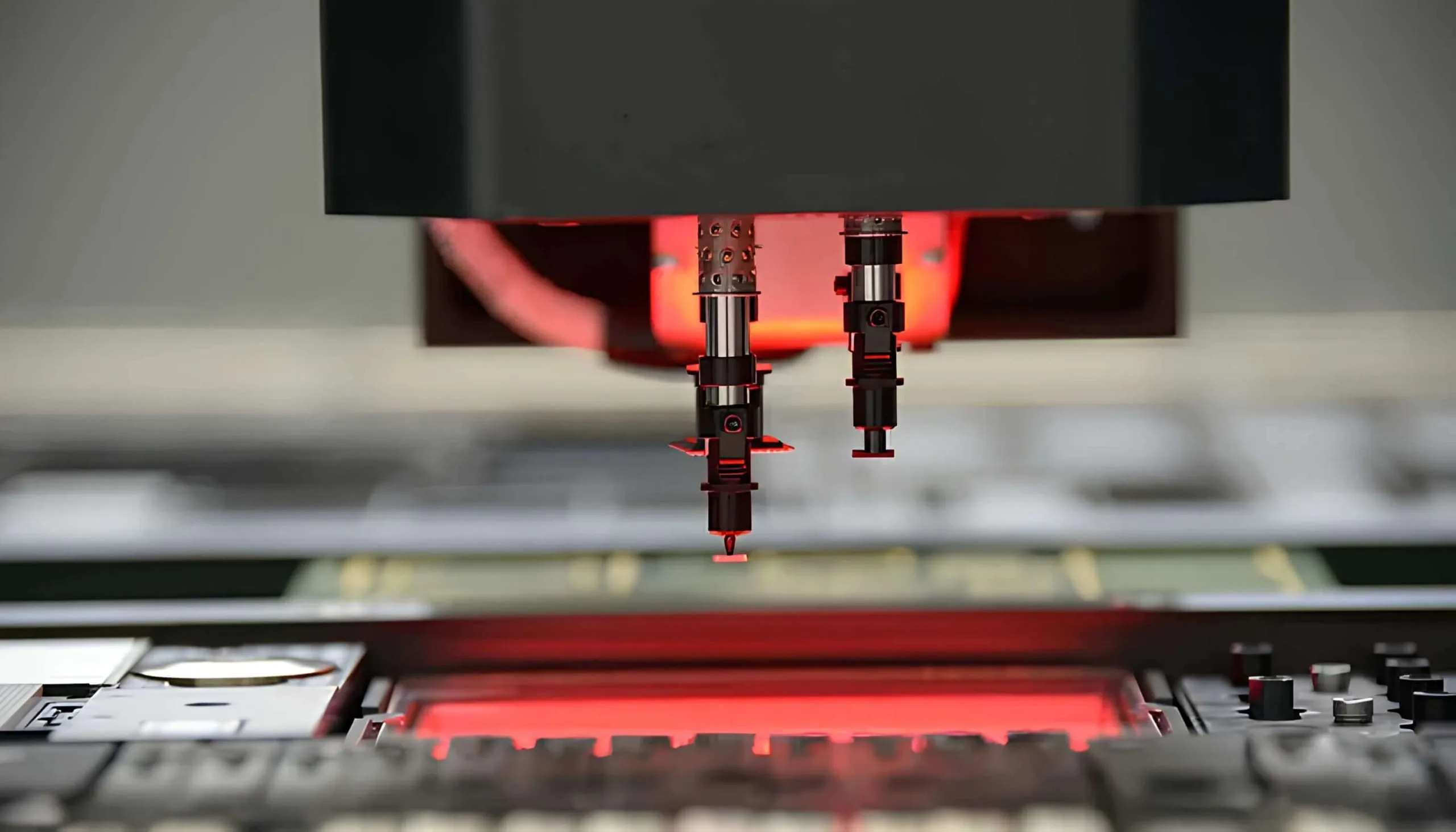
Using Cpk to Reveal the Real Accuracy of SMT Pick-and-Place Machines
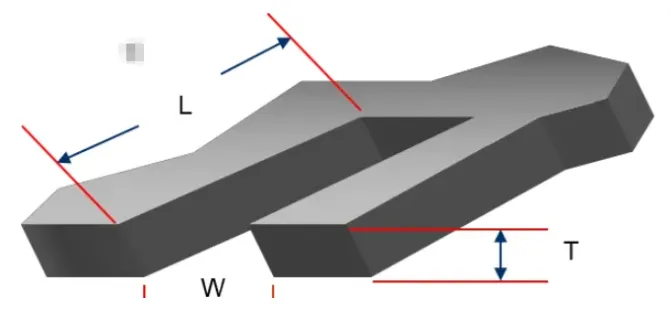
SMT Stencil Design Demystified: A Practical Guide to IPC-7525B
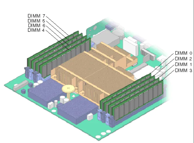
Why You Should Not Place Components Larger Than 3216 Directly Under a BGA
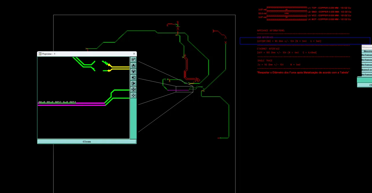
How PCB CAM Resolves Conflicting Impedance Control Requirements

Why Do Eye Diagrams Collapse Even When High-Speed Interface Traces Are Length-Matched?
Detailed Analysis of DDR Topologies
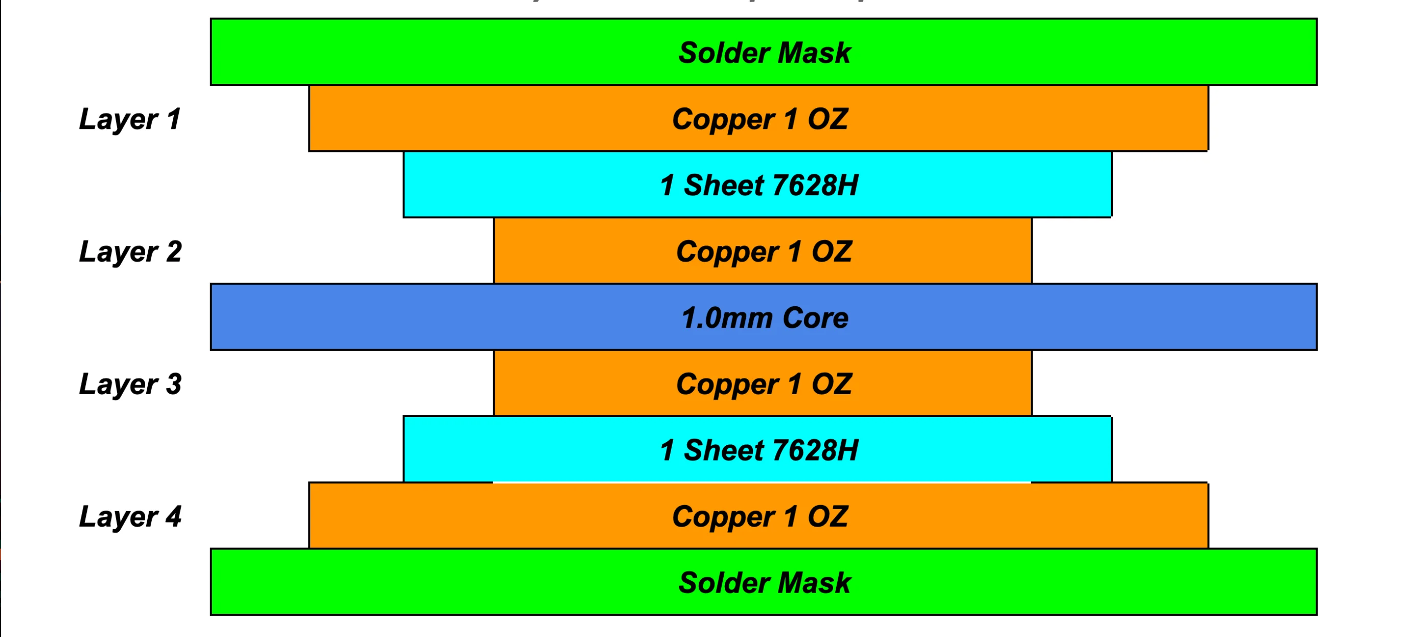
PCB CAM Review to Overcome Complex Stackup and Lamination Challenges
DFM Manufacturability Checks and Recommendations for PCBs
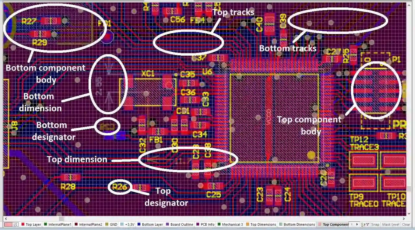
Fast Component Alignment in Altium Designer for Cleaner PCB Layouts

Understanding PCB Loss Curves: Separate the Two Variables First

Revealing the "Pseudo Eight-Layer" Stackup: Can a Six-Layer PCB Deliver Eight-Layer Performance?

PCB Layout and Routing Requirements for PCIe Interfaces

FR4 PCB Manufacturing: Materials, Process, and Fabrication Guide
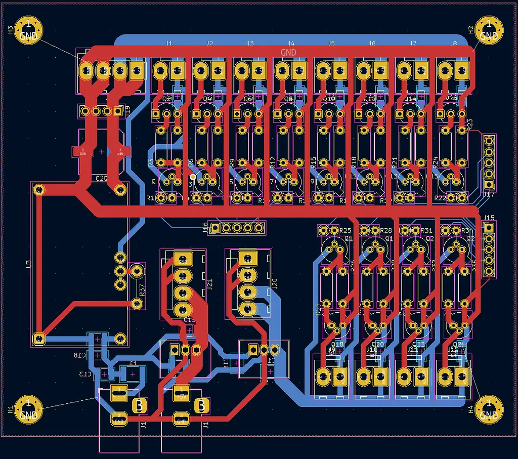
Five Most Common PCB Design Pitfalls—and How to Prevent Them
How a Series Resistor on a PCB Improves Signal Integrity