Introduction
Gerber files serve as the foundational blueprint for printed circuit board manufacturing, translating complex PCB designs into precise instructions for fabrication houses. These files capture every layer of the board, from copper traces to solder masks and silkscreens, ensuring accurate reproduction of the engineer's intent. In the PCB industry, Gerber files remain the de facto standard due to their open, ASCII-based vector format that supports high precision and compatibility across tools. Electric engineers rely on them to bridge design software outputs with manufacturing processes, minimizing errors that could lead to costly respins. Understanding the Gerber file format explained, along with generation and verification steps, empowers engineers to deliver production-ready data efficiently.
What Are Gerber Files and Why Do They Matter?
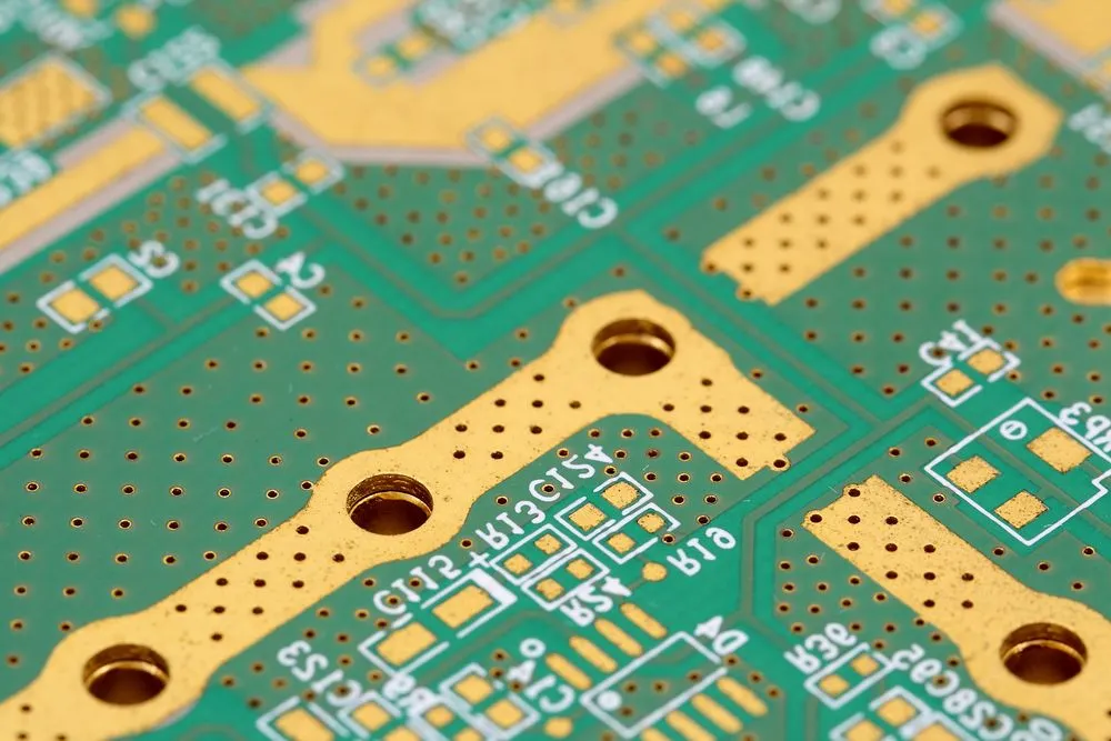
Gerber files define the two-dimensional images for each physical layer of a PCB, such as top copper, bottom copper, solder mask, and paste layers. Engineers generate separate Gerber files for each layer, accompanied by Excellon drill files for vias and holes, forming a complete data package for fabrication. This modular approach allows manufacturers to process layers independently during photoplotting, etching, and drilling stages. Without accurate Gerber files, discrepancies arise between design and production, potentially violating quality specifications like those in IPC-6012E for rigid printed boards.
The relevance stems from Gerber's universality; nearly all PCB fabricators accept this format, making it indispensable for global supply chains. For electric engineers, mastering Gerber files ensures designs meet tolerances for trace widths, clearances, and impedances critical in high-frequency applications. Poorly prepared files lead to issues like misaligned layers or missing apertures, delaying prototypes and increasing costs. Thus, Gerber files matter as the reliable conduit from simulation to silicon, upholding manufacturing integrity.
Gerber File Format Explained
The Gerber file format uses an ASCII, human-readable structure with commands prefixed by percentages for settings and coordinates for drawing primitives like lines, arcs, and flashes. Key elements include the file header with %FS* for format specification, defining resolution and polarity, followed by aperture definitions via %ADD* commands that describe shapes like circles or rectangles used for pads and traces. Coordinates follow in absolute or incremental modes, with D-codes for actions such as interpolate (D01), flash (D03), or move (D02). The format supports embedded apertures in RS-274X, eliminating the need for separate aperture lists common in the obsolete RS-274D.
Engineers appreciate the precision of RS-274X, which specifies units in inches or millimeters and resolutions up to 0.00001 inches for fine-pitch components. Commands like %LPD* set light plot dark for positive images, while %MOMM* declares metric coordinates. Each file ends with M02* to signal completion. This structured syntax enables direct interpretation by CAM software, ensuring traces and pads align perfectly across multilayer stacks.
Gerber File Standards
Gerber files adhere to the extended RS-274X specification, the industry benchmark for layer imaging data transfer in PCB manufacturing. This standard incorporates essential features like aperture embedding, coordinate formats, and step-and-repeat capabilities, promoting interoperability. While Gerber dominates, alternatives like IPC-2581 emerge for intelligent data exchange, bundling stackups and netlists in XML, yet RS-274X persists for its simplicity and tool support.
Compliance with Gerber file standards ensures files meet fabrication tolerances outlined in documents such as IPC-A-600K for board acceptability. Engineers must verify polarity, units, and offsets to avoid imaging errors during production. Adhering to these standards reduces rejection rates and aligns with quality systems like ISO 9001:2015.
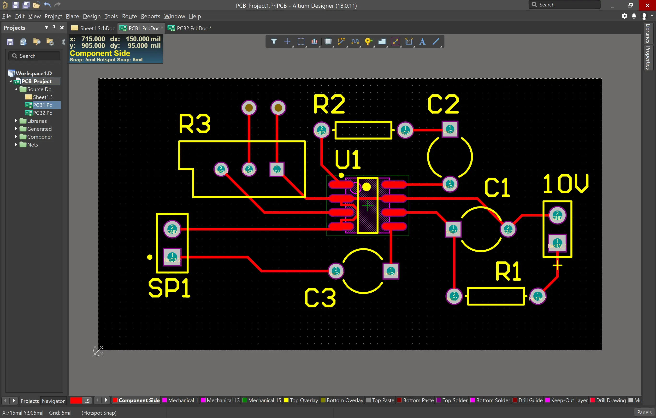
Generating Gerber Files from Altium
Generating Gerber files from Altium involves opening the PCB document in the project, then navigating to File, Fabrication Outputs, and selecting Gerber Files to launch the setup dialog. Configure the general tab for RS-274X format, inches or millimeters, and precision settings matching design rules, typically 3:5 or 3:6 for most applications. On the layers tab, enable all required layers including copper, solder mask, silkscreen, paste, and mechanical outline, while excluding non-fabrication layers like keep-out.
Proceed to the drill tab for NC drill files in Excellon format, segmented or plated options as needed, and generate apertures if not embedded. Review the output path and filename extensions, such as .GTA for top copper, then execute to produce the ZIP package. Post-generation, inspect files for completeness using a Gerber file viewer to confirm layer registration and data integrity. This workflow ensures Altium designs translate seamlessly to manufacturing.
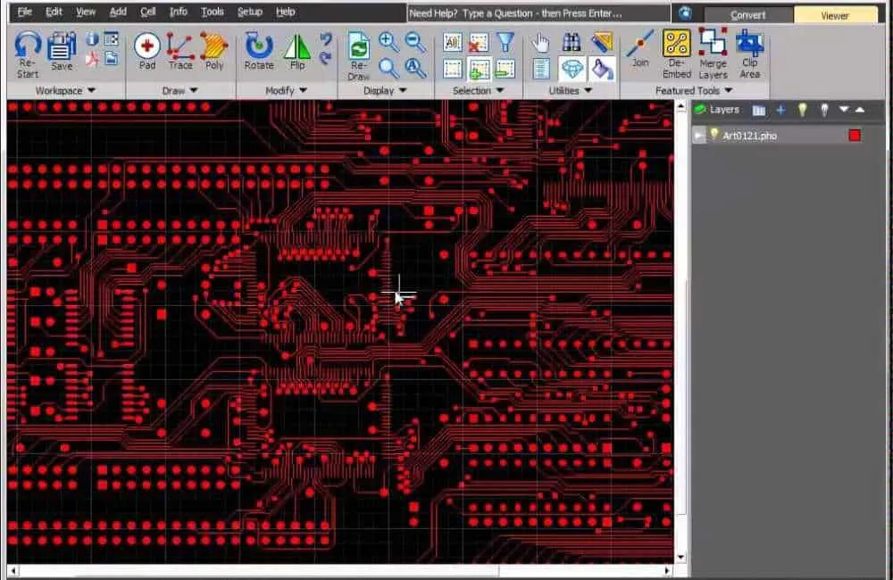
Using a Gerber File Viewer
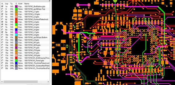
A Gerber file viewer loads and overlays multiple Gerber and drill files, simulating the final board stackup for visual inspection. Engineers stack layers transparently to check alignment of traces, pads, and vias, zooming into critical areas like BGA fanouts or high-density interconnects. Viewers display apertures, polarities, and measurements, flagging issues like overlapping masks or undersized clearances. Free options support RS-274X fully, rendering flashes and arcs accurately.
Select a viewer compatible with your OS, import the ZIP or individual files, and toggle layers on-off for targeted review. Measure distances between features to verify design rules, and export images for documentation. Regular use prevents downstream errors, saving time in prototyping cycles.
Troubleshooting Gerber File Errors
Troubleshooting Gerber file errors starts with identifying common pitfalls like missing board outline layers, which cause undefined panelization boundaries during fabrication. Empty or zero-sized files often result from unselected layers in the export dialog, while corrupted data appears as jagged lines or incomplete apertures. Mismatched units between files lead to scaling issues, and using RS-274D instead of RS-274X omits embedded apertures, forcing manual CAM corrections.
Ambiguous filenames, such as generic .GBR extensions without layer indicators, confuse processors; adopt conventions like TOP_COPPER.GBR. Layer registration errors manifest as offsets between top and bottom, verifiable in a Gerber file viewer by overlaying mechanical layers. Regenerate files after verifying design completeness, and cross-check drill hits against copper pads. Persistent issues may trace to software settings, requiring updated output configurations.
Best Practices for Gerber Files
Adopt RS-274X exclusively for all exports to leverage embedded apertures and modern features, ensuring compatibility with automated CAM flows. Include a comprehensive set: all copper layers, both solder masks, silkscreen if annotated, paste for stencil, mechanical outline, and drill files with separate plated/non-plated. Name files descriptively, e.g., F_Cu.gbr for front copper, and zip them with a readme detailing stackup and materials.
Always validate outputs in a Gerber file viewer before submission, measuring key dimensions and confirming no voids in soldermask. Reference IPC-6012E specifications during review to align imaging with performance criteria for rigid boards. Document any non-standard features in accompanying notes to guide fabricators.
Conclusion
Gerber files encapsulate the precision of PCB design for reliable manufacturing, with the RS-274X format providing robust vector descriptions of every layer. Engineers benefit from structured generation processes, viewer inspections, and error troubleshooting to deliver flawless data packages. Adhering to Gerber file standards and best practices minimizes risks, ensuring boards meet IPC quality benchmarks. Mastering these elements streamlines workflows from design to production.
FAQs
Q1: What is the Gerber file format explained in simple terms?
A1: The Gerber file format is an ASCII vector standard describing PCB layers via commands for apertures, coordinates, and flashes. RS-274X embeds all necessary data, supporting high-resolution imaging for copper traces, masks, and silkscreens. It remains the de facto choice for its readability and universality in manufacturing.
Q2: How do you generate Gerber files from Altium?
A2: Open the PCB file, go to File > Fabrication Outputs > Gerber Files, set RS-274X format and units, select layers and drill options, then generate. Verify completeness in a Gerber file viewer post-export. This ensures all design data transfers accurately.
Q3: What are common troubleshooting Gerber file errors?
A3: Frequent issues include missing layers, RS-274D usage, ambiguous names, and alignment offsets. Use a Gerber file viewer to overlay and measure, regenerating with correct settings. Proper naming and validation prevent most problems.
Q4: What Gerber file standards should engineers follow?
A4: Prioritize RS-274X for embedded features, aligning with IPC-6012E for fabrication quality. Viewers confirm compliance before submission.
References
IPC-6012E — Qualification and Performance Specification for Rigid Printed Boards. IPC, 2017
IPC-A-600K — Acceptability of Printed Boards. IPC, 2020
ISO 9001:2015 — Quality Management Systems. ISO, 2015