Introduction
In the competitive world of electronics engineering, PCB design cost often represents a substantial portion of the overall project budget. Engineers face the challenge of balancing performance requirements with manufacturing realities, where poor layout decisions can lead to escalated PCB layout cost through increased material usage, lower yields, and extended production times. Design for manufacturing cost, or DFM for PCB cost, emerges as a critical strategy to address these issues. By incorporating smart PCB layout techniques early in the design phase, teams can achieve cost-effective PCB design without compromising reliability or functionality. This approach not only streamlines fabrication and assembly but also enhances scalability for volume production. Ultimately, mastering these techniques empowers electric engineers to deliver optimized boards that meet tight budgets and deadlines.
What Is Design for Cost in PCB Layout and Why It Matters
Design for cost in PCB layout refers to the intentional application of principles that minimize manufacturing expenses while adhering to performance specifications. It integrates DFM for PCB cost guidelines from the schematic stage through final routing, focusing on factors like material efficiency, process simplicity, and yield improvement. This methodology differs from pure performance-driven design by prioritizing manufacturability alongside electrical integrity. In practice, it involves selecting layout strategies that align with standard fabrication capabilities, reducing custom tooling needs and defect rates.
The relevance of cost-effective PCB design cannot be overstated in today's market. Manufacturing expenses often stem from inefficiencies such as excessive layer counts or suboptimal routing, which inflate PCB design cost by demanding specialized processes. Poor layouts increase scrap rates and rework, directly impacting PCB layout cost and project timelines. For electric engineers, embracing these techniques ensures designs transition smoothly from prototype to production, supporting cost predictability and supplier flexibility. Industry standards like IPC-2221C provide foundational guidelines for such optimizations, emphasizing producibility levels that balance cost and quality.
Core Technical Principles Driving Cost Reduction
Several engineering principles underpin cost-effective PCB layouts, starting with material utilization. Fewer layers reduce core and prepreg consumption, a primary driver of PCB design cost, while maintaining signal integrity through careful partitioning. Board dimensions play a pivotal role; non-standard sizes complicate panelization, leading to material waste and higher setup fees. Symmetry in layout prevents warpage during lamination and reflow, avoiding costly yield losses from mechanical stress.
Routing efficiency forms another cornerstone. Minimizing via counts and trace lengths conserves copper and drilling resources, directly lowering PCB layout cost. Adhering to standard clearances and annular rings per established guidelines enhances etch yields by reducing bridging or opens. Copper balance across layers mitigates plating variations, ensuring uniform thickness and preventing delamination risks. These principles collectively enable DFM for PCB cost by aligning design with fabrication tolerances.
Drill optimization follows logically from routing choices. Using fewer, larger standard hole sizes streamlines tooling and reduces cycle times in production. Overly dense via fields strain mechanical processes, elevating expenses through extended drill wear and alignment challenges. Thermal management considerations, such as avoiding excessive copper asymmetry, further support cost goals by preventing post-fabrication failures.
Practical PCB Layout Techniques for Minimizing Expenses
Optimizing Board Outline and Panelization
Standard rectangular outlines facilitate efficient panelization, maximizing the number of boards per production panel and slashing per-unit PCB design cost. Engineers should target dimensions that fit common panel formats, avoiding irregular shapes that necessitate routing tabs or custom scoring. V-scoring or tab routing enables high-volume depanelization without individual board handling premiums.
Incorporating breakaway tabs with fiducials ensures precise alignment during assembly, reducing setup times. Mouse bites in corners provide clean separation while preserving panel integrity. These techniques enhance material utilization rates, directly impacting DFM for PCB cost effectiveness.
Strategic Component Placement
Placing components in functional groups minimizes interconnect lengths, cutting trace and via demands. Positioning high-speed signals near connectors reduces crosstalk risks and routing complexity, contributing to cost-effective PCB design. Symmetry around the board center prevents warpage by balancing thermal expansion coefficients during lamination.
Orienting parts uniformly aids automated pick-and-place, avoiding rotation penalties in assembly. Keeping edge clearances adequate for routing tools prevents mechanical damage. These placement strategies lower PCB layout cost by simplifying downstream processes.
Efficient Routing and Trace Management
Employing orthogonal routing with smooth 45-degree bends avoids etch undercuts, improving yield and reducing PCB design cost. Prioritizing wider traces for power distribution accommodates plating variations without thinning. Differential pairs should maintain consistent spacing to meet impedance targets without excessive vias.
Autorouting tools, constrained by DFM rules, accelerate layout while preserving manufacturability. Avoiding nested islands in pours prevents trapped chemicals during fabrication. These methods ensure robust signal integrity at minimal expense.
Via and Drill Optimization
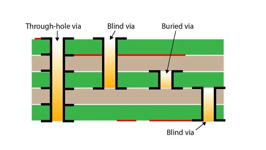
Limiting vias to essential transitions and using standard diameters consolidates drill schedules, cutting tooling costs. Staggered via patterns distribute loads evenly, enhancing mechanical reliability. Blind or buried vias, while useful for density, escalate expenses; reserve them for multilayer necessities.
Teardrops at via-to-trace junctions prevent lift-off during thermal cycling. Grouping holes by size streamlines production sequencing. Such optimizations directly lower PCB layout cost through process efficiency.
Layer Stackup and Copper Balancing
Selecting standard stackups with symmetric builds equalizes CTE stresses, per IPC-6012F qualification requirements. Balancing copper weight between layers via pours or planes avoids bow and twist, reducing test rejects. Ground planes on outer layers shield signals while aiding heat dissipation.
Thinner dielectrics enable tighter coupling but demand precise control; thicker cores suit cost-sensitive designs. These choices align with IPC-A-600M acceptability criteria, ensuring boards pass inspection without rework.
Advanced DFM Checks and Validation
Running design rule checks against IPC-2221C producibility levels catches issues early. Simulating warpage via finite element analysis predicts mechanical risks from asymmetry. Gerber reviews confirm panel fit and scoring accuracy.
Collaboration with fabrication partners refines tolerances without over-specifying. These steps embed DFM for PCB cost into the workflow, yielding predictable outcomes.
Conclusion
Smart PCB layout techniques transform design for cost from concept to reality, delivering substantial savings in PCB design cost and PCB layout cost. By prioritizing panelization, placement symmetry, routing efficiency, and standard features, engineers achieve DFM for PCB cost without performance trade-offs. Adhering to guidelines like those in key IPC standards ensures compliance and reliability. Electric engineers who integrate these practices early gain a competitive edge, enabling scalable, budget-conscious production. Ultimately, cost-effective PCB design fosters innovation by freeing resources for core functionality.
FAQs
Q1: How does component placement affect PCB design cost?
A1: Strategic placement groups related components to shorten traces and vias, reducing material and fabrication time. Symmetry prevents warpage, avoiding yield losses during lamination. Uniform orientation supports automated assembly, cutting labor expenses. This approach embodies cost-effective PCB design principles for reliable outcomes.
Q2: What role does panelization play in DFM for PCB cost?
A2: Panelization maximizes board yield per sheet, minimizing waste and setup fees. Standard rectangular shapes with V-scoring enable efficient depanelization in volume runs. Fiducials ensure alignment, streamlining inspection. These techniques directly lower PCB layout cost while maintaining quality.
Q3: Why minimize vias in cost-effective PCB design?
A3: Excessive vias increase drilling cycles and via fill demands, inflating expenses. Standard sizes consolidate tooling, enhancing throughput. Staggering prevents alignment errors. Fewer vias simplify routing, boosting etch yields and reducing PCB design cost overall.
Q4: How do IPC standards support PCB layout cost reduction?
A4: Standards like IPC-2221C guide clearances and stackups for producibility. IPC-A-600M defines acceptability to minimize rejects. They promote designs matching common processes, cutting custom work. This integration drives DFM for PCB cost efficiency.
References
IPC-2221C — Generic Standard on Printed Board Design. IPC, 2023
IPC-A-600M — Acceptability of Printed Boards. IPC, 2025
IPC-6012F — Qualification and Performance Specification for Rigid Printed Boards. IPC, 2023