Introduction
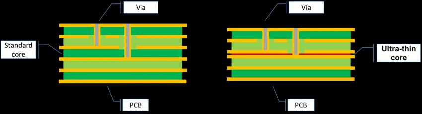
Ultra-thin printed circuit boards, typically with total thicknesses under 0.4 mm, enable compact designs in high-speed applications like 5G modules, AI accelerators, and wearable electronics. These boards support dense routing and reduced parasitics, but their geometry introduces severe signal integrity challenges. Signal integrity in thin PCBs demands precise control to prevent distortions that degrade performance at frequencies above 1 GHz. Thinner dielectrics increase capacitance between traces, lowering characteristic impedance and heightening crosstalk risks. Engineers face trade-offs between miniaturization and reliable signal transmission. This guide provides structured insights into managing these issues through proven engineering practices.
Why Signal Integrity Matters in Ultra-Thin PCBs
Signal integrity ensures that electrical signals maintain their intended shape, timing, and voltage levels from source to receiver. In ultra-thin PCBs, the reduced board thickness compresses signal paths, amplifying interactions that cause reflections, noise, and attenuation. High-frequency performance of thin PCBs suffers when uncontrolled impedance leads to mismatches, resulting in overshoot, ringing, or eye closure in serial links. Crosstalk becomes prominent due to minimal separation between adjacent traces, coupling unwanted energy between channels. For electric engineers designing multi-gigabit interfaces, neglecting these effects can cascade into bit error rates exceeding acceptable thresholds. Adhering to standards like IPC-2221 for design guidelines helps mitigate such risks systematically.
The relevance extends to flexible circuits, where dynamic bending further stresses signal paths. Thin substrates in flex designs lower loop inductance but increase sensitivity to mechanical deformation-induced discontinuities. Procurement teams specify ultra-thin boards for space-constrained products, yet manufacturing tolerances must align with performance needs. Ultimately, robust signal integrity enables higher data rates and reliability in next-generation systems.
Core Technical Principles Affecting Signal Integrity
Characteristic impedance forms the foundation of signal integrity in thin PCBs. Defined as Z0 equals the square root of inductance per unit length over capacitance per unit length, Z0 drops in ultra-thin boards because thinner dielectrics boost capacitance while proximity to ground planes reduces inductance. Engineers calculate Z0 using trace width, thickness, dielectric height, and material constants like dielectric constant (Dk). At high frequencies, skin effect confines current to conductor surfaces, raising effective resistance and insertion loss. Dielectric losses from dissipation factor (Df) also contribute, particularly in thin layers where field concentrations intensify.
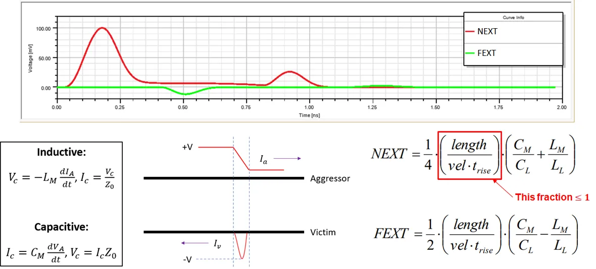
Crosstalk arises from mutual capacitance and inductance between parallel traces. In ultra-thin designs, minimal dielectric separation heightens near-end and far-end crosstalk, injecting noise that skews timing margins. The coupling coefficient scales inversely with spacing-to-height ratio, making wide spacing critical yet challenging in dense layouts. Electromagnetic interference from external sources couples more efficiently due to lower shielding effectiveness in thin stacks.
Reflections occur at impedance discontinuities like vias, bends, or terminations. Return loss quantifies this, with mismatches causing voltage standing wave ratios that distort waveforms. In high-speed designs, via stubs in thin boards act as resonant cavities, exacerbating ringing. Transmission line theory guides analysis, emphasizing matched lengths and controlled geometries.
Loss mechanisms dominate high-frequency performance of thin PCBs. Conductor loss increases with frequency due to skin depth decreasing proportionally to the square root of frequency. Thin copper foils, common in ultra-thin boards, offer limited cross-section for current flow, accelerating attenuation. Dielectric absorption in polymer resins adds phase distortion, critical for multi-gigabit signals.
Practical Solutions for Impedance Control in Ultra-Thin PCBs
Impedance control for ultra-thin PCBs starts with stackup optimization. Symmetric builds with thin cores and prepregs maintain uniform dielectric heights, targeting 50 ohms single-ended or 100 ohms differential. Engineers adjust trace widths narrower for lower Z0 in thin dielectrics, balancing with spacing rules from IPC-2141. Manufacturing tolerances on copper etch and dielectric thickness demand statistical modeling for yield. Test coupons on panels verify Z0 via time-domain reflectometry during fabrication.
Material selection influences control precision. Low-Dk, low-Df laminates minimize variations, though ultra-thin formats limit options. Hybrid stacks combining rigid and flex sections require interface transitions with impedance tapers. Simulation tools model field distributions, predicting Z0 across frequencies.
Via design mitigates discontinuities. Blind or buried vias shorten stubs in thin stacks, reducing reflections. Back-drilling, though challenging in ultra-thin boards, removes unused stub lengths. Staggered via fields in dense arrays preserve Z0 continuity.
Crosstalk Reduction Techniques in Flexible Circuits
Crosstalk reduction in flexible circuits demands aggressive spacing amid bending stresses. Minimum trace-to-trace gaps scale with dielectric thickness, often below 0.1 mm in polyimide flex. Guard traces grounded at multiple points shield aggressor-victim pairs, shunting coupled noise. Differential routing pairs tightly coupled traces, rejecting common-mode crosstalk.
Length matching minimizes far-end coupling time windows. Serpentine patterns equalize delays without excessive bends that strain flex materials. Ground stitching vias along edges form return current fences, containing fields. Standards like IPC-6013 qualify flex performance under flex cycles, ensuring integrity post-bending.
Shielding layers in multi-layer flex add reference planes, tightening field confinement. However, thin copper limits current capacity, requiring wider pours. Simulations quantify peak noise voltage, guiding iterative spacing adjustments.
Grounding Techniques for Ultra-Thin PCBs
Grounding techniques for ultra-thin PCBs prioritize low-impedance return paths. Full ground planes on inner layers provide uniform references, minimizing loop area. In single-layer flex, hatched grounds balance mechanical flexibility with electrical integrity. Via stitching every few millimeters connects planes, suppressing slot resonances.
Partitioned grounds separate analog and digital domains, preventing noise coupling. Split planes under high-speed traces require careful bridging to avoid impedance bumps. Power-ground pairs form stripline structures, enhancing decoupling.
Thermal vias in ground planes aid heat dissipation without compromising integrity. Qualification per IPC-2221 verifies planar integrity post-lamination.
Troubleshooting Common Issues in High-Speed Thin PCB Designs
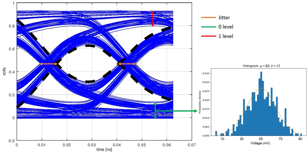
Engineers often encounter eye closure from cumulative jitter in ultra-thin boards. De-embedding test fixtures isolates board contributions during validation. Excessive insertion loss signals material or etch issues; cross-section analysis reveals copper thinning.
Crosstalk spikes post-assembly indicate bond wire interactions in stacked dies. Pre-layout simulations with 3D solvers predict these, allowing redesign. Warpage in thin flex during reflow induces microcracks; controlled ramp rates per JEDEC standards prevent this.
Conclusion
Mastering signal integrity in ultra-thin PCBs requires integrated design, simulation, and verification. Key strategies include precise impedance control for ultra-thin PCBs, crosstalk reduction in flexible circuits via shielding, and robust grounding techniques. High-frequency performance of thin PCBs improves with adherence to layered principles and standards. Electric engineers achieve reliable high-speed designs by balancing physical constraints with electromagnetic fundamentals. Implementing these practices ensures robust performance in demanding applications.
FAQs
Q1: What challenges arise in signal integrity in thin PCBs at high speeds?
A1: Signal integrity in thin PCBs degrades due to higher capacitance from thin dielectrics, leading to lower impedance and increased reflections. Crosstalk intensifies from close trace proximity, while losses rise from skin effect in thin copper. Engineers address this through controlled geometries and simulations, maintaining eye openings for multi-Gbps links. Standards guide tolerance stacks for repeatability.
Q2: How do you achieve impedance control for ultra-thin PCBs?
A2: Impedance control for ultra-thin PCBs involves stackup design with thin, uniform dielectrics and adjusted trace widths. Target Z0 by modeling field solver tools, incorporating etch and thickness variations. Fabricate test structures for TDR verification. Symmetric builds prevent warpage-induced shifts, ensuring consistency across panels.
Q3: What are effective crosstalk reduction methods in flexible circuits?
A3: Crosstalk reduction in flexible circuits uses increased spacing, guard traces, and differential routing. Ground stitching confines fields during flexing. Simulations predict coupling coefficients, optimizing layouts. IPC guidelines ensure reliability under repeated bends.
Q4: Why are grounding techniques critical for ultra-thin PCBs?
A4: Grounding techniques for ultra-thin PCBs provide low-inductance returns, minimizing noise and EMI. Planes and stitching vias form shields, essential in thin stacks with limited layers. Partitioning prevents cross-domain coupling. Proper implementation supports high-frequency performance of thin PCBs without added thickness.
References
IPC-2221B — Generic Standard on Printed Board Design. IPC, 2012
IPC-2141A — Design and Assembly Process Implementation for Embedded Components. IPC, 2005
IPC-6013DS — Qualification and Performance Specification for Flexible and Rigid-Flex Printed Boards. IPC, 2018


