Introduction
In high-volume PCB manufacturing, design for manufacturability high volume becomes essential to achieve cost efficiency and reliability at scale. Small design oversights can lead to widespread defects, escalating production costs and delaying market entry. Factory processes prioritize repeatability, where adhering to proven guidelines ensures consistent yields across thousands of units. Engineers must integrate DFM early to align designs with fabrication and assembly capabilities. This guide explores key strategies, drawing from established industry practices to optimize outcomes. By focusing on these elements, teams can minimize rework and enhance overall production flow.
High-volume runs demand robust designs that withstand automated processes like high-speed drilling, plating, and reflow soldering. Variations in material behavior or layout asymmetries amplify issues such as warpage or shorts when scaled. Proactive DFM reduces scrap rates and supports lean manufacturing principles. Factories rely on standardized checks to verify compliance before full runs. Ultimately, effective DFM transforms potential bottlenecks into streamlined operations.
What Is DFM for High-Volume PCB Manufacturing and Why It Matters
Design for manufacturability high volume refers to the systematic approach of creating PCB layouts that facilitate efficient, defect-free production in large quantities. It encompasses guidelines for layout, materials, and documentation to match factory capabilities. In high-volume contexts, DFM shifts focus from prototype flexibility to process stability, where even minor tolerances impact yield percentages. Factories process panels of multiple boards simultaneously, making panel-level optimization critical. Without DFM, issues like inconsistent plating or mask misalignment compound across batches.
DFM matters because high-volume manufacturing amplifies the cost of defects. A single design flaw, such as inadequate via annular rings, can cause opens or shorts in thousands of units, leading to recalls or downtime. It directly influences yield rates, cycle times, and total ownership costs. Standardized DFM practices ensure designs meet performance specs under real-world fabrication variations. For electric engineers, mastering DFM means bridging design intent with factory realities, resulting in reliable end products.
Adhering to IPC-2221 guidelines for conductor sizing and clearances provides a foundation for these efforts. High-volume production often targets IPC Class 2 requirements, balancing reliability with manufacturability. This class accommodates minor cosmetic imperfections while ensuring functional integrity. Engineers benefit from higher throughput and lower per-unit costs through such alignments.
Key Technical Principles of DFM in High-Volume Production
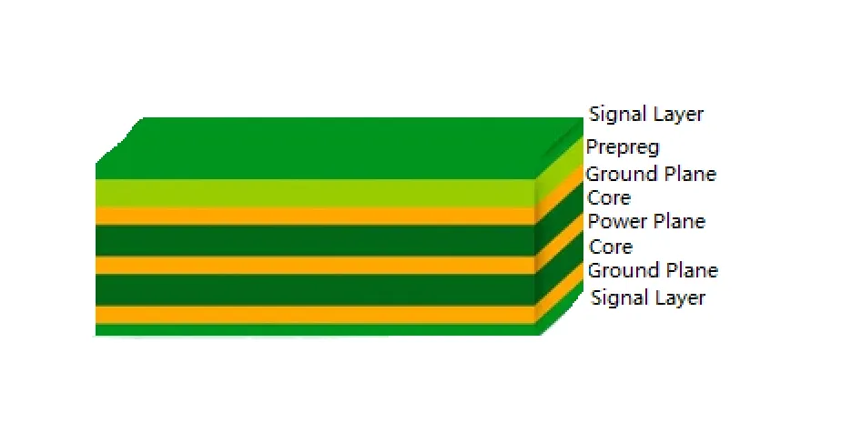
Core DFM principles revolve around layer stackup symmetry to prevent warpage during lamination and reflow. Balanced copper distribution across layers minimizes thermal stresses, a common cause of board twist in multilayer boards. Factories recommend core and prepreg pairings that match coefficients of thermal expansion. Asymmetric builds lead to dimensional instability, particularly in panels exposed to repeated thermal cycles. Proper stackup planning starts with material selection suited to the application's thermal profile.
Trace routing follows principles of adequate width and spacing to handle current without excessive heating, as outlined in established design standards. Sharp angles should be avoided to reduce etch undercuts and potential shorts. Factories emphasize copper-to-edge clearances to facilitate routing and depaneling without chipping. These rules ensure signal integrity and mechanical robustness in dense layouts.
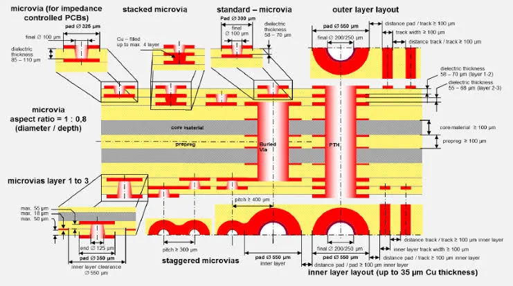
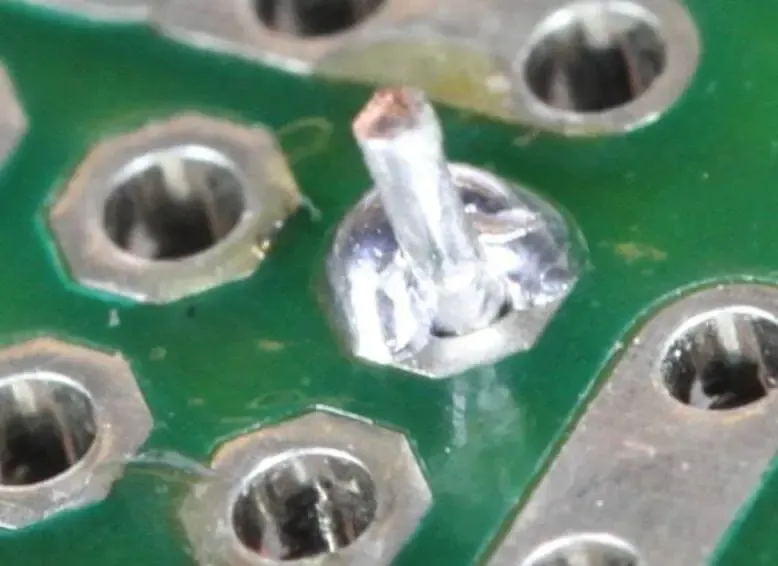
Via design principles prioritize aspect ratios suitable for plating uniformity, typically limiting depth-to-diameter ratios to prevent voids. Annular rings must provide sufficient land for interconnection without breakout risks. In high-volume, through-hole vias dominate for cost-effectiveness, while blind or buried types require additional process controls. Factory insights stress drill-to-copper clearances to account for plating buildup.
Material choices influence DFM by ensuring compatibility with high-speed processes. Substrates with controlled glass transition temperatures resist delamination under reflow peaks. Factory-driven validation includes coupons for dielectric integrity. These principles collectively support scalable production.
DFM Checklist PCB: Essential PCB Design Rules High Volume
A comprehensive DFM checklist PCB guides engineers through critical verification steps before submission. Start with complete file sets, including Gerber layers, drill files, netlists per IPC formats, and stackup drawings. Verify all layers align without offsets, as misregistration causes alignment defects in volume runs. Include fiducials and tooling holes for precise panel handling and automated assembly.
Layer stackup rules demand symmetry, with equal dielectric thicknesses on both sides of the core. Alternate signal layers with planes to control impedance and EMI. Confirm copper weights match current demands without excessive thinning. Factories flag unbalanced planes as high-risk for bow and twist.
Trace and space rules require minimum clearances scaled to copper thickness and voltage levels. Ensure teardrops on narrow junctions to prevent lift-offs during etching. Maintain consistent routing densities to avoid over-etch in sparse areas. These PCB design rules high volume promote uniform plating and solderability.
Via rules specify adequate annular rings per IPC-6012 Class 2 criteria, allowing controlled breakout while ensuring connectivity. Check for slotting needs in high-aspect holes and tenting compatibility. Avoid clustering to prevent drill wander. Factory checks include aspect ratio compliance for void-free barrels.
Solder mask and silkscreen rules focus on clearances from pads and traces to prevent bridging or bleed. Define relief areas around vias and fiducials for inspection access. Silkscreen must remain legible post-reflow, with sufficient line widths and air gaps. Panelization rules optimize array spacing, v-scoring, or tab routing for depaneling efficiency.
- Files & Documentation: Gerbers, drills, netlist, BOM, stackup PDF
- Stackup: Symmetry, plane alternation, CTE match
- Traces: Width/space per current/voltage, teardrops
- Vias/Holes: Annular ring, aspect ratio, clearance
- Mask/Silkscreen: Pad clearance, legibility, reliefs
- Panel: Fiducials, scoring, array efficiency
Best Practices for Minimizing PCB Defects High Volume
Minimizing PCB defects high volume starts with early factory collaboration to align on capabilities. Simulate etch compensation to predict trace narrowing in inner layers. Use design rule checks tied to IPC-A-600 acceptability criteria for visual standards. These practices catch issues pre-production, preserving yields.
Address warpage by validating stackup through thermal modeling and coupon testing. Symmetric builds combined with controlled lamination ramps reduce bow below acceptable limits. Factories monitor panel flatness post-press, rejecting asymmetric designs. This prevents downstream assembly defects like tombstoning.
Plating defects like voids or thin copper arise from poor via design; enforce drill clearances and rinse cycles in specs. Netlist verification per IPC standards flags opens or shorts early. Automated optical inspection thresholds should match Class 2 tolerances.
Solder mask defects, such as webbing or non-coverage, stem from tight geometries; expand openings beyond pad extents. Silkscreen overlaps lead to reflow charring, so enforce air gaps. For high-volume, specify non-tacky inks resistant to handling.
Assembly-focused practices include land patterns per IPC-7351 to optimize solder joints. Place components away from edges for fixturing stability. These steps minimize defects like bridging or insufficient paste volume.
Common Pitfalls and Troubleshooting Insights
Unintended copper pours or hairline traces often escape DRCs, causing EMI or opens in volume runs. Factory x-ray reveals these post-plating. Solution: Flood fill selectively and verify netlists against schematics.
Mask misregistration appears as pad exposure; troubleshoot by checking layer alignment and expansion values. High-volume panels amplify this, so use reference marks.
Stubbed vias from incomplete connections plague multilayers; ensure pads on all intersecting layers. Troubleshooting involves sectioning samples for continuity checks.
Conclusion
Optimizing DFM for high-volume PCB manufacturing hinges on disciplined adherence to principles like symmetric stackups, robust via rules, and complete documentation. These practices, rooted in factory insights, directly boost yields and cut costs. Electric engineers gain by embedding DFM checklists into workflows early. PCB design rules high volume ensure scalability from prototype to production. Ultimately, proactive DFM delivers reliable boards that perform under real-world stresses.
FAQs
Q1: What is a DFM checklist PCB for high-volume manufacturing?
A1: A DFM checklist PCB verifies design elements like stackup symmetry, trace clearances, via annular rings, and mask expansions against factory capabilities. It includes file completeness and panelization rules to prevent defects. Following this checklist aligns with IPC-2221 for conductor rules, ensuring high yields in design for manufacturability high volume scenarios. Factories use it to flag issues pre-run.
Q2: Why are PCB design rules high volume critical for stackup?
A2: PCB design rules high volume emphasize symmetric layer builds to counter warpage from thermal mismatches. Balanced copper and dielectrics maintain flatness during lamination and reflow. Factories reject asymmetric stacks due to assembly fixturing failures. Adhering prevents bow exceeding IPC-6012 limits.
Q3: How does DFM minimize PCB defects high volume like shorts?
A3: DFM minimizes PCB defects high volume by enforcing trace spacings, annular rings, and etch compensation per standards. Netlist checks catch opens early, while mask clearances avoid solder bridges. Factory-driven rules like drill-to-copper gaps ensure plating uniformity, reducing shorts in panels.
Q4: What role do standards play in design for manufacturability high volume?
A4: Standards like IPC-2221 guide trace sizing and IPC-A-600 define acceptability for high-volume reliability. They provide factory-aligned tolerances for vias and masks. Integrating them ensures defect-free scaling without redesigns.
References
IPC-2221B — Generic Standard on Printed Board Design. IPC, 2003
IPC-6012E — Qualification and Performance Specification for Rigid Printed Boards. IPC, 2017
IPC-A-600K — Acceptability of Printed Boards. IPC, 2020