Introduction
In the competitive landscape of electronics manufacturing, achieving high PCB yield rates directly impacts production costs, time-to-market, and overall product reliability. Design for Manufacturability (DFM) principles serve as a foundational strategy to bridge the gap between PCB design intent and factory-floor execution. By integrating DFM guidelines for PCB yield early in the design phase, engineers can minimize defects such as opens, shorts, and warpage that plague high-volume production. This approach not only enhances PCB design for manufacturing yield but also aligns with industry expectations for robust, repeatable processes. Electric engineers familiar with layout tools understand that small oversights in spacing or material selection can cascade into significant yield losses during fabrication and assembly. Ultimately, mastering DFM transforms potential failure points into strengths, enabling smoother transitions from prototype to mass production.
Understanding DFM and Its Role in PCB Yield
Design for Manufacturability refers to the systematic consideration of manufacturing constraints during the PCB design process to optimize yield and reduce variability. In PCB contexts, DFM encompasses guidelines that address fabrication tolerances, assembly challenges, and material behaviors under processing conditions. Yield, defined as the percentage of functional boards produced from a given panel, suffers when designs exceed equipment capabilities or ignore process-induced stresses. For instance, inadequate annular rings around vias can lead to drill breakout during plating, directly lowering design for assembly PCB yield. Industry standards like IPC-2221 provide baseline rules for conductor sizing and spacing, ensuring designs remain feasible across varied fab houses. Why does this matter? Poor yield escalates scrap rates, rework costs, and delivery delays, often by factors that dwarf initial design savings.
DFM’s relevance amplifies in multilayer boards where interlayer alignment and thermal expansion mismatches amplify risks. Engineers must evaluate how design choices interact with processes like lamination, etching, and reflow soldering. High-yield designs anticipate these interactions, incorporating margins that accommodate real-world tolerances such as etch factor variations or solder paste deposition inaccuracies. Without DFM, even advanced prototypes fail in production, underscoring the need for proactive yield-focused design. This mindset shifts PCB design from artistic layout to engineered predictability, fostering confidence in scaling to volume.
Core DFM Principles for Enhancing PCB Manufacturing Yield
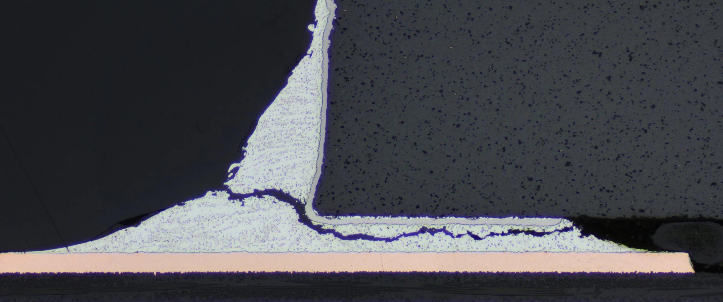
Effective DFM guidelines for PCB yield begin with conductor geometry, where trace widths and spaces must exceed minimums dictated by current density and fab capabilities. Narrow traces risk under-etching or over-etching, creating opens or shorts that compromise yield. Spacing rules prevent bridging during plating or soldering, with clearances scaled to board thickness and layer count. Vias demand special attention: blind and buried vias require precise depth control, while standard through-vias need sufficient annular rings, typically at least 0.1 mm, to withstand drill wander. Asymmetric via patterns can induce warpage, pulling panels out of flatness during reflow.
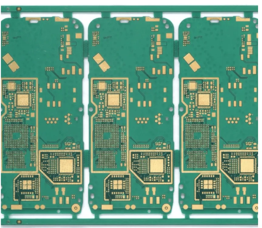
Material selection forms another pillar, balancing electrical performance with mechanical stability. Substrates with mismatched coefficients of thermal expansion (CTE) relative to copper exacerbate cracking in plated through-holes under thermal cycling. Panelization strategies further boost yield by promoting symmetry: evenly distributed coupons, fiducials, and routing tabs minimize stress gradients across arrays. Fabricators prefer designs with breakaway tabs that avoid burrs during depanelization, preserving edge quality for assembly. Adhering to these principles reduces process-induced defects, directly elevating PCB design for manufacturing yield.
Solder mask and silkscreen application represent subtle yet critical DFM facets. Overhangs less than 0.075 mm on pads invite tenting failures, exposing copper to environmental hazards post-fabrication. Legend placement must avoid vias and fine-pitch components to prevent ink bleed during printing. For high-density interconnects, tented vias protect against solder wicking, maintaining joint integrity. These details, when overlooked, contribute to assembly rejects, highlighting DFM’s role in holistic yield optimization.

Implementing DFM Best Practices for Superior Yield
To apply DFM guidelines for PCB yield, start with a design review checklist aligned to fabrication flows. Verify drill sizes against standard charts, favoring common diameters like 0.3 mm or 0.4 mm to leverage existing tooling and reduce setup times. Aspect ratios for vias should not exceed 10:1 to prevent plating voids, a common yield killer in deep holes. Copper weight distribution influences etching uniformity; balanced planes prevent telegraphing effects where uneven removal distorts traces. Engineers should simulate warpage using panel symmetry tools, aiming for mirror-image layouts that counteract lamination bow.
In assembly-focused DFM, component placement optimizes for stencil printing and reflow. Fine-pitch parts demand pad geometries per IPC-7351, with toe, heel, and side fillets proportioned to prevent tombstoning or bridging. Keep reflow profiles in mind by minimizing board size variations and placing heat-sensitive components away from edges. Fiducial marks, at least 1 mm diameter with clear zones, enable precise pick-and-place alignment, boosting design for assembly PCB yield. Post-assembly inspections reveal DFM gaps, such as insufficient mask dams between pads, which allow solder shorts.
Advanced practices include specifying controlled impedance for high-speed signals, with trace widths adjusted via stackup calculators to hit target values within 10% tolerance. Edge plating or castellations require pullback distances to avoid solder wicking during wave soldering. For rigid-flex boards, bend radii and transition zones follow flex-specific rules to prevent cracking. Regularly consulting fab DFM reports refines iterative designs, closing the loop on yield improvements.
Troubleshooting Common Yield Issues Through DFM
Factory-driven insights reveal recurring yield pitfalls addressable via DFM. Warpage, often exceeding 0.75% bow/twist per IPC-6012E, stems from asymmetric copper or poor panelization. Counter this by balancing copper area within 10% across layers and incorporating stress-relief slots. Plating voids in vias arise from air entrapment; specify sequential plating and tenting to mitigate. Solder mask delamination links to poor adhesion on high-copper surfaces, resolved by specifying cross-sectioned mask with adequate buildup.
Component shifting during reflow ties to pad misdesign; enlarge pads for QFNs and use type 4 or finer paste for BGAs. Delamination in multilayers points to inadequate prepreg flow; ensure resin content matches core thickness. These troubleshooting steps, rooted in DFM, prevent escalation from prototype success to production failure. Electric engineers benefit from early fab feedback loops, refining designs pre-tapeout.
Conclusion
DFM principles stand as indispensable tools for electric engineers aiming to maximize PCB manufacturing success. By embedding DFM guidelines for PCB yield into workflows, designs evolve from viable prototypes to high-volume performers. Key takeaways include prioritizing symmetry, tolerances, and process compatibility to sidestep common defects. This proactive stance not only cuts costs but elevates reliability, aligning with the demands of modern electronics. Consistent application yields compounding benefits, from faster ramps to superior field performance. Embrace DFM as a core competency to drive unparalleled manufacturing outcomes.
FAQs
Q1: What are the key DFM guidelines for PCB yield that electric engineers should prioritize?
A1: DFM guidelines for PCB yield emphasize trace spacing, via annular rings, and panel symmetry to prevent etching defects and warpage. Engineers must adhere to minimum clearances scaled by layer count and balance copper distribution for uniform lamination. Standard drill sizes and solder mask overhangs further safeguard against plating voids and bridging. Implementing these reduces scrap by addressing fab tolerances upfront, ensuring high PCB design for manufacturing yield.
Q2: How does PCB design for manufacturing yield influence assembly processes?
A2: PCB design for manufacturing yield directly enhances assembly by optimizing pad layouts and fiducial placement for accurate stencil printing and pick-and-place. Proper component spacing avoids shadowing during reflow, minimizing tombstoning in fine-pitch devices. Edge clearances and mask dams prevent solder shorts, streamlining inspection. This integration boosts design for assembly PCB yield, cutting rework and accelerating throughput.
Q3: Why is symmetry important in DFM for preventing PCB warpage?
A3: Symmetry in DFM counteracts thermal stresses during lamination and reflow, keeping bow and twist below acceptable limits. Balanced copper areas and mirrored coupon placement distribute forces evenly across panels. Asymmetric designs induce curvature, complicating assembly and handling. Prioritizing this principle in PCB design for manufacturing yield maintains flatness, supporting reliable high-volume production.
Q4: Can DFM principles improve yield in multilayer PCBs specifically?
A4: Yes, DFM principles target multilayer challenges like interlayer alignment and CTE mismatches to elevate yield. Sequential lamination rules and via aspect ratios prevent voids and misalignment. Balanced stackups with matched materials reduce delamination risks under thermal cycling. These measures ensure robust interconnections, optimizing design for assembly PCB yield in complex boards.
References
IPC-2221G — Generic Standard on Printed Board Design. IPC, 2022
IPC-6012E — Qualification and Performance Specification for Rigid Printed Boards. IPC, 2015
IPC-A-600K — Acceptability of Printed Boards. IPC, 2020


