When the sheet metal PCB enclosure design comes across my desk, the same handful of issues keep showing up. They don't always kill the board right away, but they create headaches in assembly, reliability problems in the field, or extra cost that could have been avoided with tighter coordination between the PCB layout and the enclosure drawing.
Bend tolerances and hole positioning top the list. Engineers often treat the enclosure as a simple box without accounting for how sheet metal actually behaves during forming.
Bend Radius Effects on Internal Clearances
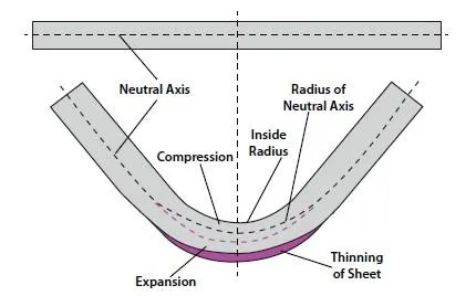
Sheet metal bends never come out perfectly sharp. Typical mild steel or aluminum enclosures use a minimum inside bend radius of 0.5 to 1 times material thickness. That radius eats into your usable internal space more than most layouts expect.
Layout guys will place components right up to the calculated wall position. Then the bend radius pushes the wall inward and suddenly the tall capacitor or connector sits 0.3mm too close. During assembly the enclosure presses against the part or the board flexes.
This shows up frequently in 1.5mm or 2mm aluminum boxes. The outer dimension looks perfect on the 3D model, but the formed part tells a different story.
Accounting for Material Springback
Springback after bending moves hole locations. Designers who lock down mounting hole positions based on flat pattern dimensions get surprised when the final folded enclosure doesn't line up.
I've seen 0.2-0.4mm shifts common on longer bends. For a PCB with tight mechanical tolerances, that misalignment puts stress on the screws and eventually on the solder joints or traces near the mounting holes.
Hole Positioning and Tolerance Stack-Up in Sheet Metal PCB Enclosure Design
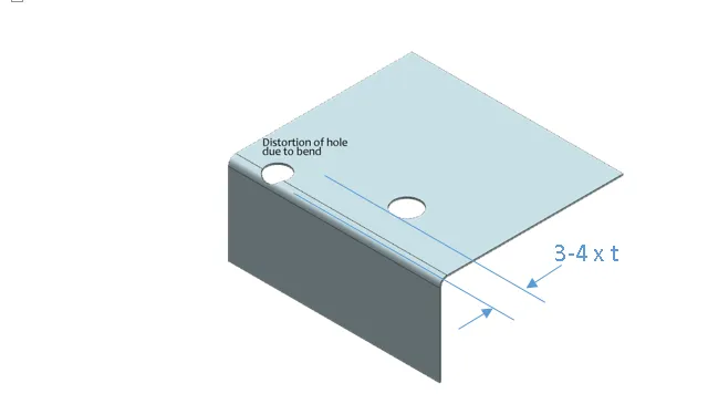
Punching holes before bending is standard, but the tolerance chain gets ugly fast. Hole-to-bend location tolerance is usually ±0.1mm to ±0.3mm depending on the shop and material. Add in PCB fab tolerance of ±0.1mm for mounting holes and you can easily end up with 0.5mm or more total mismatch.
That doesn't sound terrible until you have a connector that needs to mate through the enclosure or a board that must sit flat against multiple standoffs.

Common fix I recommend is oversizing the PCB mounting holes slightly — 0.3-0.5mm extra diameter on the board side when the enclosure uses fixed holes. Or switch to slots in one axis to absorb the variation.
Never assume the sheet metal shop will hit perfect locations. Talk to them early about datums and critical features.
Threaded Inserts and Boss Alignment
Press-in or rivet nuts seem like a good idea for thin sheet metal. The problem comes when the insert shifts during installation or the surrounding material deforms. The PCB mounting screw then pulls at an angle.
This creates uneven pressure across the board and can crack traces or lift pads over thermal cycles. Especially painful on boards with heavy components near mounting points.
Mounting Structure Choices That Stress the PCB
Rigid screw-down points without proper standoff height or compliance lead to board bow. 1.6mm FR4 isn't infinitely stiff. A few tenths of a millimeter warp from uneven enclosure pressure is enough to cause solder joint fatigue.
Common observation: enclosures designed with direct contact between sheet metal and PCB components without thermal gap or insulation. Heat from the board transfers unevenly and components near the walls run hotter.
Best practice is to design in at least 0.5mm extra clearance beyond the tallest component near enclosure walls, and verify with the actual bend radius and material thickness.
Grounding Tabs and Contact Reliability
Many enclosures rely on finger stock or bent tabs for grounding. If the tab geometry doesn't maintain consistent pressure after assembly and vibration, contact resistance goes up. That hurts both EMI performance and safety grounding.
On the PCB side, make sure the corresponding ground pads or traces are sized generously and placed where the contact actually lands after all tolerances.
EMI Shielding Gaps Created by Sheet Metal Details
Seams and holes in sheet metal PCB enclosure design are the usual leakage paths. Engineers sometimes prioritize easy assembly over continuous electrical contact. A 0.2mm gap might look fine mechanically but radiates nicely at higher frequencies.
Bends that aren't fully closed or overlapping seams without proper gasketing create slot antennas. The PCB layout then needs heavier shielding cans or more filtering to compensate.

For critical designs, I push for conductive gaskets or finger stock that maintains contact even after repeated opening. On the PCB, route sensitive traces away from enclosure seams by at least 5-10mm where possible.
Vent Hole Placement and Noise Coupling
Vent patterns look nice but if they line up with high-speed traces or clocks on the PCB, you get direct coupling. Same with display or connector cutouts.
Coordinate cutout locations with the PCB designer before finalizing the enclosure. A small shift in hole pattern can save a lot of rework on shielding or layer stack adjustments.
Practical Rules for Better Sheet Metal PCB Enclosure Design Coordination
Share the 3D step files both ways early. Don't wait until the PCB is in fab. Check bend tables and forming notes from the enclosure manufacturer.
Typical guidelines that reduce issues:
- Minimum 1mm component clearance to inside walls after bend radius
- Mounting hole tolerance compensation via slots or oversized holes on PCB
- Standoff heights verified against tallest components plus 0.5mm margin
- Ground contact areas on PCB at least 3mm diameter pads
- Keep high-speed signals 8mm+ away from enclosure seams when possible
These aren't theoretical. They come from watching boards come back with bent pins, cracked components, or failing EMC after assembly.
The best sheet metal PCB enclosure design happens when the mechanical and PCB teams talk tolerances before the first layout pass. Small adjustments in keep-out zones or hole placement prevent most of the common failures.
Next time you're laying out a board that goes into sheet metal, pull the enclosure drawing first and build the constraints in from the start. Saves time, money, and a lot of debugging later.