Introduction
In the PCB industry, Design for Manufacturing (DFM) serves as a critical strategy to enhance production efficiency while aligning with broader sustainability goals. DFM PCB sustainability focuses on creating designs that minimize material usage and streamline fabrication processes from the outset. By anticipating manufacturing constraints early, engineers can significantly reduce waste PCB manufacturing generates, such as copper scrap and chemical effluents. This approach also optimizes PCB design for energy, lowering the power demands of etching, lamination, and drilling operations. Factory-driven insights reveal that poor DFM often leads to rework, which consumes additional resources and energy. Ultimately, integrating DFM principles promotes efficient PCB production and supports environmental responsibility.
What Is DFM and Why It Matters for PCB Sustainability
Design for Manufacturing (DFM) refers to the practice of designing printed circuit boards with manufacturing capabilities in mind, ensuring seamless transition from design to production. In PCB contexts, DFM encompasses guidelines for trace widths, via placements, layer stackups, and board outlines that align with standard fabrication tolerances. This methodology directly contributes to DFM green PCB initiatives by preventing defects that cause scrap and excess energy use. For instance, non-standard features increase the risk of misalignment during drilling or etching, leading to higher rejection rates.
The relevance of DFM in sustainability stems from the resource-intensive nature of PCB production. Processes like chemical etching consume large volumes of copper and generate hazardous waste, while high-temperature lamination requires substantial energy input. Adhering to DFM reduces these impacts by maximizing yield and minimizing iterations. Electrical engineers benefit from DFM as it bridges design intent with factory realities, fostering reliable, eco-efficient outcomes. Industry standards like IPC-2221 reinforce these practices by providing generic guidelines for producible designs.
Key Technical Principles of DFM for Waste Reduction
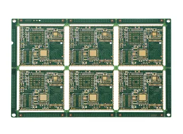
One core principle of DFM involves optimizing board geometry to fit standard panel sizes, which dramatically cuts material waste. Factories typically process PCBs in large panels, and irregular outlines lead to unusable edges that become scrap. By designing boards with dimensions that tile efficiently, such as multiples of common panel grids, engineers enable higher utilization rates. This strategy aligns with factory-driven workflows, where v-scoring or tab routing facilitates depanelization without damaging components. Balanced copper distribution across layers prevents warpage, another common waste source during cooling after lamination.
Layer stackup design plays a pivotal role in DFM PCB sustainability. Symmetric arrangements, with similar materials and thicknesses on outer layers, maintain board flatness and reduce stress during thermal cycling. Unbalanced stackups often result in bowing or twisting, necessitating rework or scrapping entire panels. IPC-6012 specifies performance requirements for rigid boards, emphasizing stackup integrity to avoid such issues. Engineers should prioritize core and prepreg selections that match thermal expansion coefficients, further minimizing defects.
Trace routing and spacing guidelines form another foundation for reducing waste. Adhering to minimum clearances prevents shorts during plating or etching, which could otherwise ruin batches. Optimized routing also shortens signal paths, indirectly supporting energy efficiency in end-use applications. Factories report that DFM-compliant routing lowers etching times by reducing excess copper removal.
Mechanisms for Energy Optimization Through DFM
DFM optimizes PCB design for energy by streamlining fabrication steps that are power-hungry. Drilling, for example, consumes significant electricity, especially with dense via arrays; DFM encourages via sharing and elimination of unnecessary holes. Fewer drills mean shorter machine run times and lower energy draw. Similarly, controlled impedance traces reduce the need for extensive testing iterations, conserving power in quality control phases.
Etching processes benefit immensely from precise DFM. Overly dense or narrow traces increase under-etch risks, prompting slower etch rates or multiple passes, both energy-intensive. Designs with adequate annular rings and uniform line widths allow faster, more uniform etching, cutting chemical recirculation pump usage. Factory insights highlight that DFM green PCB practices here can align with ISO 14001 environmental management principles by curbing energy-related emissions.
Lamination energy ties closely to material choices and stackup symmetry. Thinner cores and optimized press cycles, enabled by DFM, shorten dwell times under heat and pressure. This not only saves electricity but also reduces wear on equipment, extending service life.
Practical Best Practices for Efficient PCB Production
To reduce waste PCB manufacturing, start with panelization planning during the design phase. Use software to array boards with optimal spacing, incorporating breakaway tabs for handling. Standardize outline shapes like rectangles over irregular forms to maximize panel yield. Electrical engineers should collaborate with fabricators early to confirm routing rails and fiducials placement.
Implement balanced copper pours on each layer to combat warpage. Aim for 50-60% coverage uniformity, adjusting with fill patterns where needed. This practice, rooted in factory experience, prevents camber that complicates assembly and leads to scrap.
For energy savings, minimize layer count without compromising functionality. Combine signals on inner layers efficiently and use blind or buried vias judiciously. Select drill sizes from standard charts to avoid custom tooling, which extends setup energy.
Adopt standard trace widths and spaces per IPC guidelines, scaling with current requirements. Wider traces for power reduce resistance losses in production testing. Route high-speed signals away from edges to prevent delamination risks during depanelization.
Incorporate test points and fiducials strategically to speed electrical testing, reducing probe station energy. Factory-driven DFM also favors surface finishes like ENIG for their process efficiency over alternatives requiring more rinsing steps.
Challenges and Factory Insights in DFM Implementation
While DFM promises gains, challenges arise from conflicting design goals like high density versus producibility. Engineers must weigh miniaturization against tolerances, often iterating stackups for balance. Factories observe that initial DFM reviews catch 80% of issues, averting costly prototypes.
Thermal management intersects with sustainability; DFM ensures vias under components aid heat dissipation, potentially lowering operational energy in devices. Poor planning leads to hotspots, increasing failure rates and rework energy.
Insights from production floors stress documentation: clear fab drawings with notes on material specs prevent mismatches. Regular DFM checklists aligned with standards streamline this.
Conclusion
Design for Manufacturing (DFM) stands as a cornerstone for DFM PCB sustainability, directly tackling waste and energy in PCB production. By optimizing geometry, stackups, and routing, it minimizes scrap from warpage and misalignment while shortening energy-intensive processes. Factory-aligned practices like panelization and balanced designs yield efficient PCB production outcomes. Electrical engineers adopting these principles not only enhance reliability but also contribute to greener manufacturing. Prioritizing DFM early unlocks long-term savings and environmental benefits.
FAQs
Q1: What are the main ways DFM reduces waste in PCB manufacturing?
A1: DFM PCB sustainability reduces waste through panelization for optimal material use, symmetric stackups to prevent warpage scrap, and standard geometries that fit factory panels. Balanced copper distribution avoids bowing during lamination cooling. These practices lower rejection rates from etching defects or drilling errors. Factories emphasize early design reviews to catch issues proactively.
Q2: How does optimizing PCB design for energy via DFM work?
A2: Optimizing PCB design for energy involves minimizing vias and layers to cut drilling and lamination power needs. Uniform trace spacing enables faster etching with less chemical pumping. Standard drill sizes eliminate custom tooling energy. DFM green PCB approaches align with efficient factory cycles, reducing overall consumption.
Q3: Why is IPC-2221 important for DFM in sustainable PCB production?
A3: IPC-2221 provides generic guidelines for trace sizing, spacing, and layout that enhance producibility. It supports reduce waste PCB manufacturing by standardizing features that prevent defects. Engineers use it for stackup and material choices promoting energy efficiency. Factory insights confirm its role in higher yields.
Q4: Can DFM practices improve end-product energy efficiency?
A4: Yes, DFM efficient PCB production indirectly boosts device efficiency via shorter traces and better thermal vias. Balanced designs ensure reliable assembly, minimizing field failures that waste energy. Optimized routing reduces parasitic losses in operation.
References
IPC-2221 — Generic Standard for Printed Board Design. IPC.
IPC-6012E — Qualification and Performance Specification for Rigid Printed Boards. IPC, 2017.
ISO 14001:2015 — Environmental Management Systems. ISO, 2015.


