










Build Your PCB at AIVON: Precision Manufacturing Process from Imaging to Final Test
Key Moment
What This Video Covers
This video provides a detailed look at AIVON's PCB manufacturing process, showing exactly how engineering designs are turned into reliable, high-performance circuit boards. It reveals the critical synergy between advanced automation and expert human oversight that ensures consistent quality.
The tour highlights key production stages including high-precision Laser Direct Imaging (LDI), ultra-fast CNC drilling, lamination, etching, plating, rigorous AOI inspection, and final electrical testing. Viewers see how AIVON maintains a pristine, controlled manufacturing environment optimized for both speed and surgical accuracy across various board types.
This process is particularly valuable for engineers developing medical devices, automotive electronics, aerospace systems, and industrial control applications where reliability and signal integrity are non-negotiable. The video demonstrates why choosing a manufacturer with strong process control directly impacts product success.
Get an instant PCB quote and experience this process with your next design. For complex projects, explore our HDI PCB capabilities or full turnkey PCB assembly services.
Key Highlights
- Advanced Automation & Precision: High-precision LDI imaging and ultra-fast CNC drilling deliver exceptional accuracy across every layer.
- Zero-Defect Quality Control: Expert technicians perform rigorous AOI and electrical testing to guarantee reliability in every board.
- Human + Technology Synergy: Perfect balance of cutting-edge machinery and skilled oversight ensures uncompromising quality in PCB manufacturing.
Core Stages That Transform Design Files into Finished Boards
Design data is first verified for manufacturability before entering the imaging area. Laser Direct Imaging transfers the circuit pattern directly onto photoresist without contact masks, eliminating registration errors common in traditional phototools. Subsequent CNC drilling creates vias and component holes at high spindle speeds while maintaining positional accuracy across the panel.
Lamination bonds the imaged cores under controlled heat and pressure to form multilayer stacks. Etching removes unwanted copper, and plating builds copper thickness inside holes and on surface features. Each transition is monitored for residual contamination, copper uniformity, and dimensional stability. Final boards undergo full electrical testing to confirm continuity and isolation before shipment.
These sequential steps illustrate why process capability data, rather than isolated machine specifications, determines whether a board will perform reliably in the field.
Laser Direct Imaging and High-Speed CNC Drilling Accuracy
Laser Direct Imaging systems project the circuit pattern with sub-micron positioning accuracy. This capability is essential for fine-line designs and HDI constructions where traditional film tooling introduces stretch and misalignment. Real production data shows that LDI reduces outer-layer registration variation compared with contact exposure methods, directly lowering the risk of annular ring violations and trace-to-pad shorts.
CNC drilling follows with optimized feed rates and bit geometries matched to material type and hole size. Entry and exit material selection, stack height, and vacuum extraction are controlled to prevent burrs, nail-heading, and resin smear. Inadequate control at this stage commonly produces incomplete plating or reliability failures under thermal cycling.
DFM practice requires designers to observe minimum drill-to-copper clearances and preferred aspect ratios so that the drilling process remains inside the equipment's proven process window.
Lamination, Etching, and Plating Controls for Layer Integrity
Multilayer lamination requires precise control of temperature ramp, pressure profile, and vacuum level to achieve void-free bonding and uniform dielectric thickness. Deviations produce resin starvation, delamination, or warped panels that later fail electrical test or assembly.
Etching chemistry and conveyor speed are adjusted to the copper weight and feature size so that undercut remains within tolerance. Over-etching reduces conductor width and current-carrying capacity; under-etching leaves residual copper bridges. Plating baths are continuously monitored for copper concentration, additive levels, and agitation to ensure consistent hole-wall thickness and surface distribution.
Failure to maintain these parameters is a frequent root cause of open vias, thin copper, and impedance variation in high-speed designs.
Automated Optical Inspection and Electrical Testing Protocols
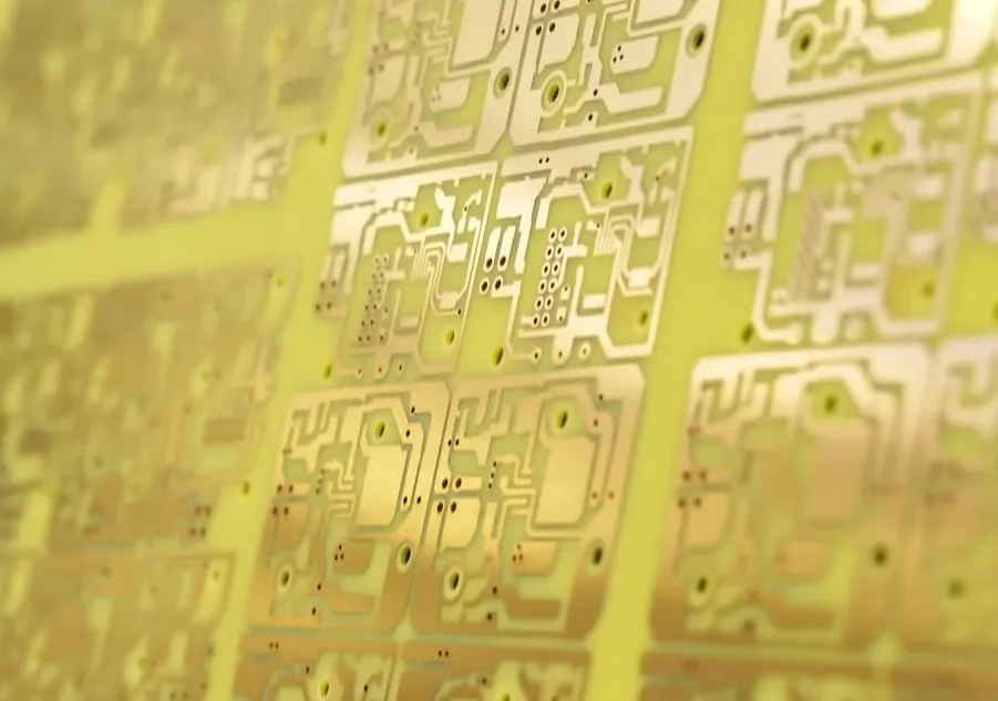
After patterning and plating, every panel passes through Automated Optical Inspection that compares the finished artwork against the original design data. AOI detects opens, shorts, missing features, and dimensional deviations at a resolution unattainable by manual inspection. Suspect locations are reviewed by trained technicians before the panel advances.
Electrical testing then verifies continuity of every net and isolation between adjacent conductors. Flying-probe or fixture-based testers apply programmed voltage and current limits to identify latent opens or resistive shorts. Boards that fail either inspection are quarantined for root-cause analysis rather than reworked and released.
This dual verification sequence is the primary mechanism that converts process capability into measured zero-defect outgoing quality.
Critical Process Controls That Prevent Common PCB Failures
Real production experience shows that the majority of field returns originate from a small set of controllable process deviations. Layer-to-layer misregistration during lamination creates annular-ring breakout and reduces via reliability under thermal stress. Insufficient desmear after drilling leaves resin residue that prevents proper copper adhesion, resulting in intermittent opens. Plating thickness variation produces high-resistance vias that fail under high current or temperature cycling.
Surface preparation before solder-mask application is equally critical. Residual oxides or organic contamination cause solder-mask adhesion loss and subsequent corrosion. Controlled micro-etch depth, cleanliness verification, and immediate processing after preparation eliminate this failure mode.
Designers can further reduce risk by providing complete fabrication notes that specify copper weights, material types, and critical tolerances. When these notes align with the manufacturer's process capabilities, the probability of latent defects drops significantly.
Environmental and Material Handling Requirements for Consistent Yield
Temperature, humidity, and particulate control inside the imaging, lamination, and plating areas directly affect dimensional stability and defect density. Photoresist sensitivity and copper surface oxidation rates change with ambient conditions; therefore the facility maintains tight environmental envelopes. Material handling protocols prevent panel edge damage, copper scratching, and contamination from human contact.
Prepreg and core materials are stored under controlled conditions and conditioned before lay-up to stabilize moisture content. Uncontrolled moisture leads to delamination and blistering during subsequent thermal processes. These environmental and handling disciplines are invisible in a finished board yet account for a measurable portion of yield variation across different fabricators.
DFM Alignment Between Design Intent and Production Reality
Successful conversion of a design into a reliable board requires that the layout respect the statistical process windows of the actual equipment. Minimum trace and space values must allow for the etch factor and registration tolerance of the imaging and etching processes. Drill sizes and annular rings must accommodate positional accuracy of the CNC machines and subsequent plating thickness.
Impedance-controlled designs benefit from documented stack-up tolerances and material dielectric constant ranges rather than nominal values alone. When designers request capabilities that sit at the extreme edge of a process, yield and reliability both decline. Early collaboration on stack-up, material selection, and critical feature tolerances converts theoretical performance into production-capable designs.
Practical Process Parameter Reference
| Process Stage | Key Control Parameter | Typical Production Window | Common Failure if Outside Window |
|---|---|---|---|
| Laser Direct Imaging | Registration accuracy | ±15 µm or better | Annular ring breakout, shorts |
| CNC Drilling | Positional accuracy / hole quality | ±50 µm / burr-free | Incomplete plating, resin smear |
| Lamination | Temperature / pressure profile | Material-specific ramp rates | Delamination, voids, warpage |
| Copper Plating | Hole-wall thickness uniformity | ≥25 µm average, min 20 µm | High-resistance vias, opens |
| AOI / Electrical Test | Defect detection threshold | Design-rule based | Escape of latent opens or shorts |
FAQ
Q1: What quality control measures does AIVON use during PCB manufacturing?
A1: Every board undergoes Automated Optical Inspection (AOI) and full electrical testing, backed by expert technician review at critical stages to achieve zero-defect standards.
Q2: How does AIVON ensure both speed and precision in PCB production?
A2: Through a combination of high-precision LDI imaging, automated CNC drilling, and a highly optimized production line managed in a pristine controlled environment.
Q3: Can AIVON handle complex multilayer and HDI PCBs?
A3: Yes. Our manufacturing process is fully equipped for multilayer, HDI, rigid-flex, and high-frequency boards with tight tolerances and advanced material support.
Q4: What DFM issues most frequently affect LDI and drilling yield?
A4: Insufficient copper-to-edge clearance, aggressive aspect ratios, and unaccounted registration tolerances are the leading causes of reduced yield. Providing complete fabrication notes and observing recommended design rules keeps features inside the proven process window.
Q5: How does environmental control influence multilayer reliability?
A5: Stable temperature, humidity, and cleanliness prevent moisture-related delamination, photoresist variation, and surface contamination that otherwise produce latent defects after thermal cycling or humidity exposure.
Welcome to AIVON, where your designs come to life through engineering excellence. Quality begins in our pristine, controlled environment, housing the industry's most advanced automated machinery.
From high-precision LDI imaging to ultra-fast CNC drilling, our facility is optimized for both speed and surgical accuracy. But technology is only half the story. Our expert technicians oversee every stage, performing rigorous AOI and electrical testing to ensure zero-defect reliability.
At AIVON, we don't just manufacture boards; we engineer the high-performance heart of your technology. Witness the perfect synergy of human expertise and advanced automation. This is how we build your PCB—with uncompromising quality, every single layer.





