










Fast, Reliable & Precise PCB Manufacturing Process
Key Moment
What This Video Covers
This video takes you inside AIVON's advanced PCB manufacturing facility, showcasing how we combine high-speed automation with rigorous engineering standards to produce superior printed circuit boards. You'll see our high-speed CNC drilling machines creating precise holes with exceptional accuracy, followed by automated solder mask and developing lines that ensure clean, sharp traces and a flawless, burr-free finish.
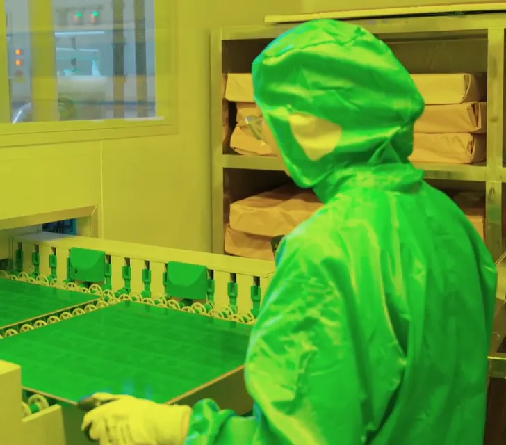
Every stage operates in an immaculate, ultra-clean environment to eliminate contamination and variables, resulting in reliable PCBs with excellent signal integrity and thermal management. The video highlights our ability to maintain rapid throughput while upholding the highest quality standards for demanding applications.
Whether you need FR4 PCBs for standard applications, high-frequency PCBs using Rogers materials for RF designs, or rigid-flex PCBs for compact, flexible solutions, our process ensures consistent performance. Engineers and procurement teams trust AIVON for PCB prototype runs and PCB mass production alike, particularly in critical sectors such as medical devices, automotive, and aerospace.
Key Highlights
- Automated Precision Drilling & Processing: High-speed CNC drilling combined with fully automated solder mask lines delivers perfectly sharp traces and burr-free edges in a controlled cleanroom environment.
- Speed Without Compromise: Advanced robotics and optimized workflows enable rapid PCB fabrication while maintaining strict engineering standards for reliability and signal integrity.
- Cleanroom Manufacturing Excellence: Every board benefits from contamination-free production, ensuring high-performance results suitable for aerospace, medical, and industrial control systems.
High-Speed CNC Drilling Accuracy Across Multilayer Stacks
High-speed CNC drilling remains one of the most critical operations in achieving a fast, reliable & precise PCB manufacturing process. Modern multi-spindle machines operate at rotational speeds exceeding 150 000 rpm while maintaining positional accuracy typically within ±0.025 mm or better. In multilayer constructions the registration between layers must stay within tight limits; any misalignment creates annular-ring breaks or via-to-trace shorts that only appear after plating and electrical test.
Tool wear is monitored continuously through spindle-load sensors and automatic bit-change systems. When a drill bit exceeds its recommended hit count, hole-wall quality degrades, leading to rough plating surfaces and subsequent reliability failures under thermal cycling. Production data show that automated bit management reduces scrap related to hole quality by more than 40 % compared with manual tool changes.
For HDI and microvia designs the same platforms switch to laser drilling or hybrid mechanical-laser sequences. The video illustrates how the transition between mechanical and laser steps is handled without breaking the cleanroom chain, preserving the low particle counts required for high-density interconnects. Designers who specify drill sizes and aspect ratios within the equipment capability windows (typically ≤10:1 for mechanical drills on standard FR4) obtain both the speed and the first-pass yield that the process is engineered to deliver.
Automated Solder Mask Application for Sharp, Burr-Free Traces
After imaging and etching, the solder-mask stage determines both cosmetic quality and long-term reliability. Fully automated curtain-coating or spray systems deposit a uniform dry-film or liquid photoimageable mask with thickness variation held to ±5 µm. Precise registration of the mask artwork relative to the copper features prevents solder-mask bridges or openings that can cause shorts or insufficient solder-wetting during assembly.
Developing and curing parameters are tightly controlled. Under-cured mask can delaminate under reflow temperatures; over-cured mask becomes brittle and cracks during flexure or thermal shock. The automated line shown in the video maintains continuous feedback on exposure energy, developer concentration, and oven temperature profiles, eliminating the batch-to-batch variation common in manual or semi-automated processes.
Burr-free edges are achieved by combining optimized etch chemistry with controlled mask thickness. Residual copper burrs or mask residue act as stress concentrators and can initiate dendritic growth in humid environments—failure modes that are particularly unacceptable in medical and aerospace electronics. The cleanroom environment surrounding the mask line further reduces the probability of particulate inclusion under the cured mask, a defect that often escapes visual inspection yet causes latent field failures.
Ultra-Clean Production Controls That Protect Signal Integrity
Contamination control is not an optional enhancement; it is a core requirement for a fast, reliable & precise PCB manufacturing process. Particle counts, ionic cleanliness, and electrostatic discharge (ESD) levels are monitored at every critical station. Even microscopic dust can embed itself in plated through-holes or under solder mask, creating intermittent opens or impedance discontinuities that degrade high-frequency performance.
Humidity and temperature stability inside the clean zones prevent moisture absorption in prepreg and core materials. Excess moisture leads to delamination or measling during lamination and subsequent reflow. Real production data consistently show that boards processed under ISO Class 5–7 conditions exhibit measurably higher insulation resistance and lower residual ion levels after cleaning.
For RF and high-speed digital designs the same cleanliness directly translates into tighter control of dielectric constant and loss tangent. Rogers or other low-loss laminates are especially sensitive to surface contamination; the video demonstrates how these materials move through the line without exposure to uncontrolled ambient air, preserving the electrical properties specified by the designer.
Throughput and Consistency from Prototype to Volume Runs
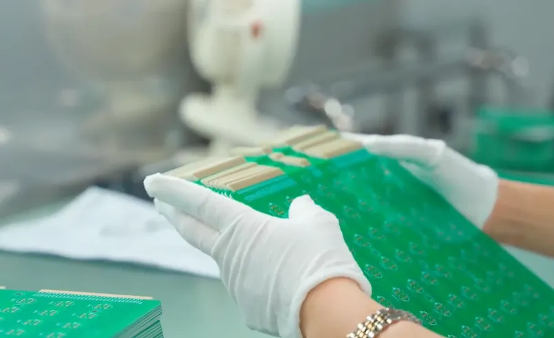
The same process platforms and control systems serve both quick-turn prototypes and sustained production volumes. Change-over times between different panel sizes, layer counts, and material types are minimized through recipe-driven automation rather than manual setup. This eliminates the classic trade-off between speed and quality that occurs when prototype and production lines are physically or procedurally separated.
Statistical process control (SPC) data collected at drilling, plating, and mask stages are applied uniformly regardless of lot size. Consequently, the first articles of a prototype run exhibit the same capability indices as the thousandth panel of a production order. Designers therefore receive consistent feedback on manufacturability and can lock DFM rules earlier in the design cycle.
Common Process Risks Avoided Through Automation and Cleanroom Discipline
| Process Stage | Typical Manual Risk | Automated + Cleanroom Mitigation | Impact on Final Board |
|---|---|---|---|
| CNC Drilling | Bit wear, positional drift, debris retention | Real-time load monitoring, auto bit change, vacuum extraction | Reduced open vias, improved plating adhesion |
| Solder Mask Application | Thickness variation, misregistration | Closed-loop coating, vision alignment | Elimination of mask bridges and insufficient coverage |
| Developing & Curing | Under/over exposure, residual chemistry | Continuous chemistry monitoring, precise thermal profiles | Prevention of delamination and ionic contamination |
| Overall Cleanliness | Particle and ESD events | Continuous particle monitoring, ESD flooring & ionizers | Higher insulation resistance, lower field failure rate |
FAQ
Q1: How does automation improve PCB manufacturing quality and speed?
A1: Automation, particularly high-speed CNC drilling and robotic solder mask application, significantly reduces human error, ensures consistent precision across batches, and accelerates production cycles while maintaining tight tolerances required for multilayer and HDI PCBs.
Q2: What makes a cleanroom environment important for PCB fabrication?
A2: A controlled ultra-clean environment eliminates dust and contaminants during critical stages like etching, plating, and lamination. This results in better yield rates, improved reliability, and superior electrical performance — essential for medical devices, aerospace, and high-frequency applications.
Q3: Can AIVON handle both prototype and production volumes with the same quality?
A3: Yes. Our flexible production ecosystem supports quick-turn PCB prototypes as well as high-volume manufacturing with identical precision standards, process controls, and quality assurance throughout.
Q4: What drill aspect-ratio limits should designers observe to maintain high yield in high-speed CNC processes?
A4: For standard FR4 multilayer boards, mechanical drill aspect ratios are typically kept at or below 10:1. Exceeding this limit increases the risk of broken bits, incomplete plating, and reduced annular-ring integrity. When higher ratios are required, sequential laser or hybrid drilling is employed while remaining inside the same clean production flow.
Q5: How does residual ionic contamination affect long-term reliability, and how is it controlled?
A5: Residual ions promote electrochemical migration and dendritic growth under bias and humidity. Automated cleaning stations followed by resistivity-of-solvent-extract (ROSE) or ion-chromatography testing keep contamination levels well below industry thresholds (typically <1.56 µg/cm² NaCl equivalent). Boards that pass these controls demonstrate substantially longer mean time between failures in harsh environments.
At AIVON, we've engineered a production ecosystem where speed and precision coexist. Our facility showcases the pinnacle of automated manufacturing.
Witness the relentless efficiency of our high-speed CNC drilling and the meticulous accuracy of our automated solder mask and developing lines. Every stage is optimized within an immaculate, ultra-clean environment to eliminate variables. The result? High-performance PCBs featuring perfectly sharp traces and a flawless, burr-free finish that speaks to our quality.
By harmonizing advanced robotics with rigorous engineering standards, we ensure rapid throughput without compromising integrity.
This is AIVON: Fast. Reliable. Precise. That's how we make your PCBs.





