 00:39
Solder Mask Application
Solder mask application is a critical process in printed circuit board (PCB) manufacturing, serving as the protective coating that shields copper traces from oxidation, prevents solder bridges during assembly, and enhances the overall durability of the board. For engineers, hobbyists, and manufacturers searching for insights on this topic, understanding solder mask application can significantly improve PCB reliability and performance. This tag encompasses a range of articles that delve into the fundamentals, from selecting the right type of solder mask—such as liquid photoimageable (LPI) or dry film—to mastering application techniques like screen printing, curtain coating, or spray methods. One key benefit of exploring solder mask application is gaining practical knowledge to avoid common pitfalls, such as uneven coverage or adhesion issues that can lead to electrical shorts or environmental degradation. For instance, ensuring proper surface preparation, including thorough cleaning of the PCB substrate, is essential for optimal mask adhesion and longevity. Best practices include controlling curing temperatures and times to achieve the desired hardness and chemical resistance, which are vital for boards exposed to harsh conditions in automotive or aerospace applications. Articles under this tag often highlight real-world case studies, where precise application has reduced failure rates in high-volume production. Whether you are troubleshooting defects like mask peeling or seeking ways to integrate solder mask into automated assembly lines, the content here offers actionable steps tailored to various skill levels. By reviewing these resources, you can refine your processes, such as using UV exposure for photoimageable masks to create fine-pitch features, ultimately leading to more efficient and cost-effective PCB designs. This collection serves as a valuable reference for optimizing solder mask application in your projects, with in-depth discussions on materials, equipment, and industry standards to support informed decision-making.
Video Guide
Technical Articles
SMT PCB Dimensional Expansion and Shrinkage: Root Causes and Mitigation Strategies for Process Engineers

Why the Solder Mask Bridge Disappears Even When There Is a Gap Between Pads
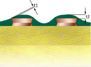
PCB Solder Mask Thickness: When It Is Too Thick, It Becomes Armor; When It Is Too Thin, It Creates Hidden Risks

Copper Base PCB CAM Review: Key Manufacturing Adjustments

Plug-and-Print or Plug First, Then Print? Comparing PCB Via-Plugging Processes

Why Does Immersion Tin Cause Solder Mask Peeling?

PCB Manufacturing Pre-Treatment Processes and Their Functions

Which PCB Solder Mask Pretreatment Should You Choose?

How to Prevent Ink Residue Inside NPTH Holes

PCB Solder Mask Openings and Solder Mask Dams: Design Intent and Manufacturing Considerations
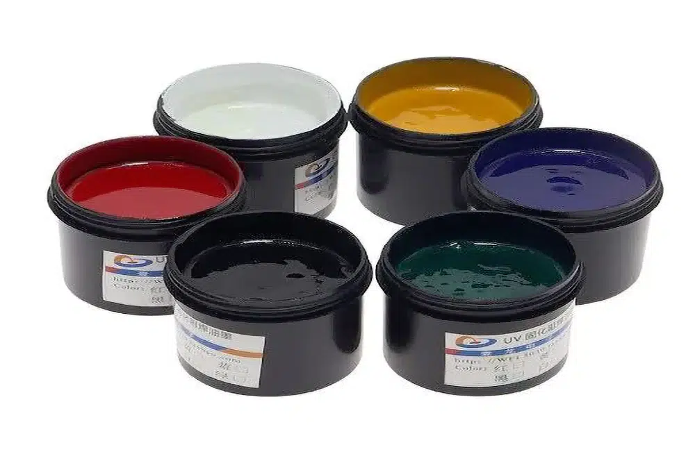
DIY Solder Mask Application: A Simple Guide for Electronics Enthusiasts
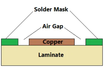
Rigid PCB Solder Mask: Protecting Your Board and Improving Solderability
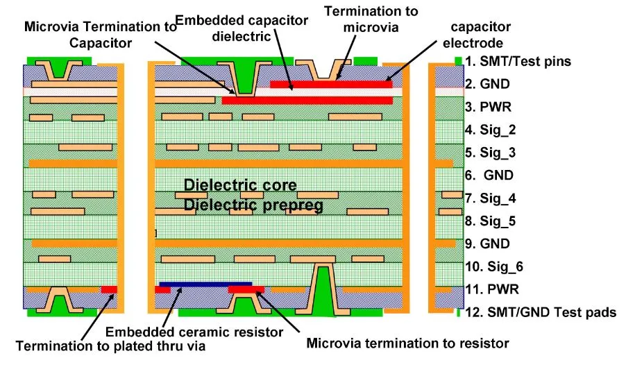
How PCB Manufacturers Improve Solder Mask Yield in HDI Production
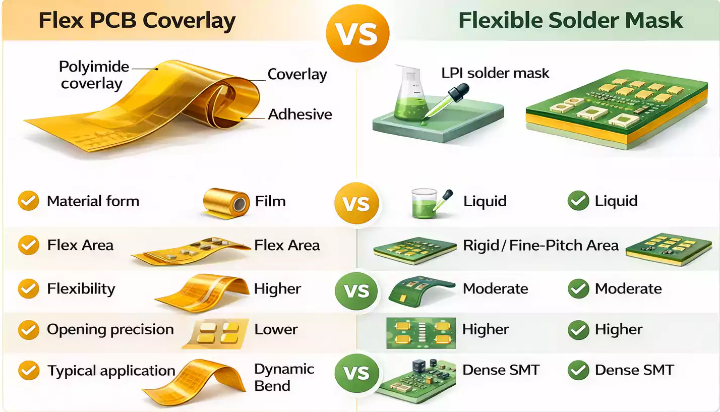
Coverlay Opening vs Solder Mask Opening: What's the Difference?

How Do FPC Factories Compensate Coverlay Openings in Practice?
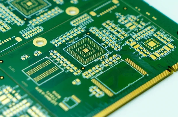
The Ultimate Guide to Selecting the Right Dry Film Solder Mask Thickness for Optimal PCB Performance
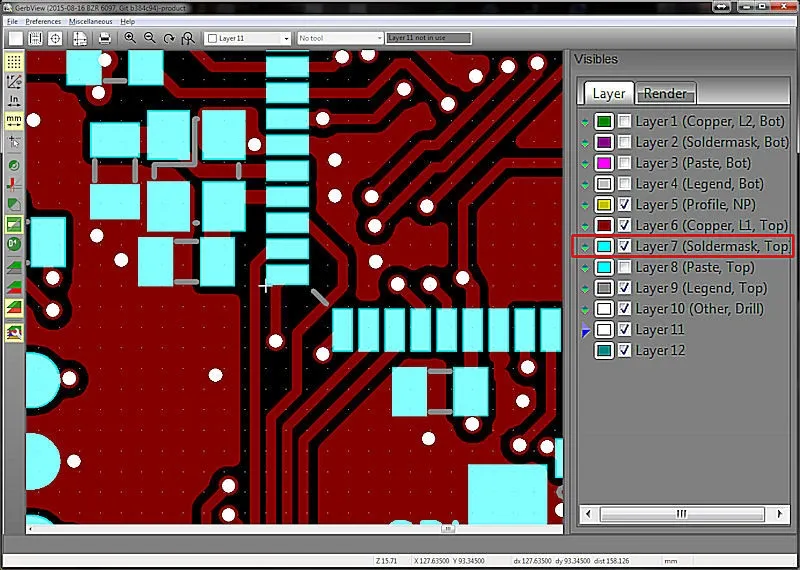
How to Specify Solder Mask Colors in Your Gerber Files
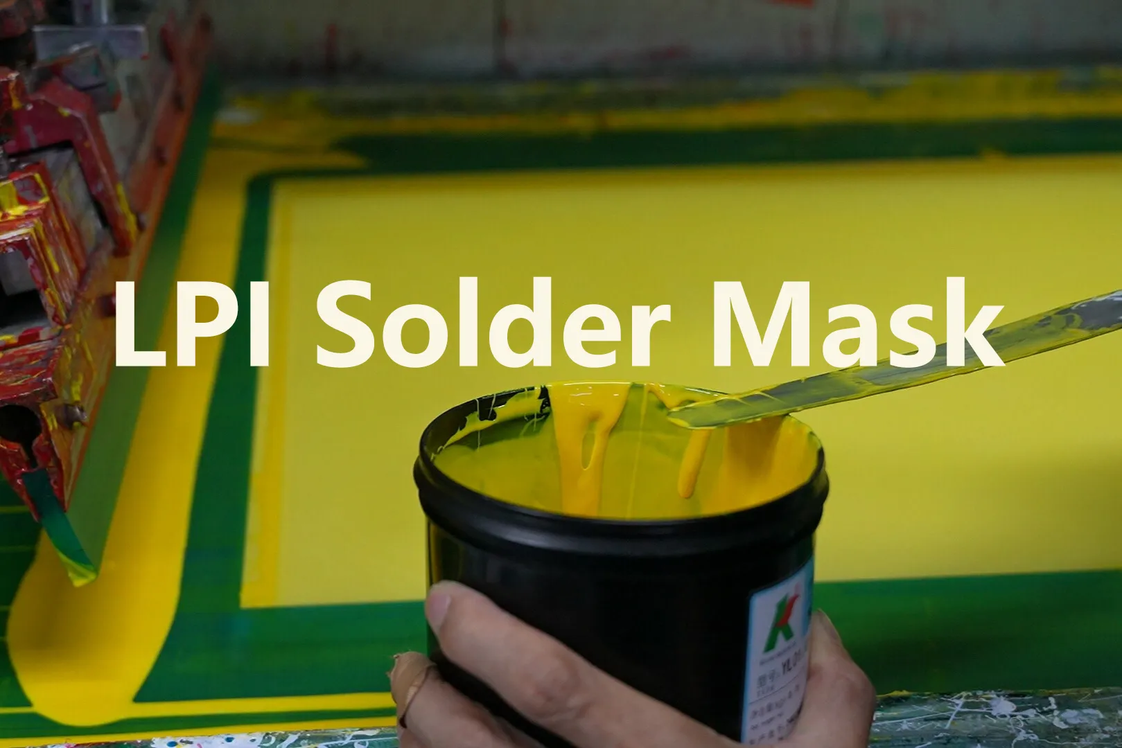
Advanced Liquid Photoimageable Solder Mask Techniques for Fine Line PCBs
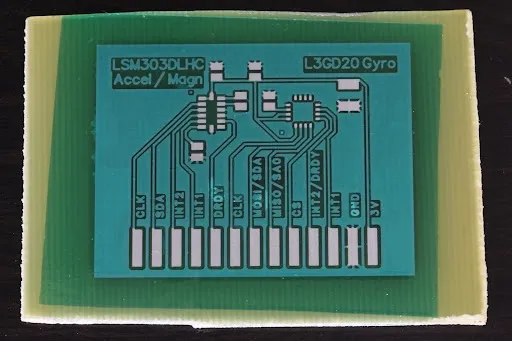
Mastering the Dry Film Solder Mask Exposure Process: A Step by Step Tutorial