Introduction
Solder mask serves as a vital protective layer on printed circuit boards, shielding copper traces from environmental damage and preventing unintended solder bridges during assembly. For electronics hobbyists embarking on DIY PCB projects, applying solder mask at home elevates homemade boards from basic prototypes to more reliable, professional-looking circuits. This guide focuses on simple, accessible methods that require minimal equipment, making it ideal for beginners in the electronics space. Whether you are building custom sensors or audio amplifiers, understanding solder mask application enhances PCB durability and performance. Hobbyists often overlook this step, but it significantly reduces shorts and oxidation over time. With basic supplies like UV lamps and liquid masks, you can achieve results close to factory standards right in your workshop.
What Is Solder Mask and Why It Matters for DIY PCBs
Solder mask is a thin polymer coating applied over the copper layers of a PCB, leaving pads and vias exposed for soldering. It acts as an insulator, protecting traces from moisture, dust, and corrosion while preventing solder from flowing where it should not during assembly. In DIY electronics, this layer is crucial for hobbyists who hand-solder components, as it minimizes bridging risks on dense boards. Without solder mask, bare copper oxidizes quickly, leading to poor solder joints and unreliable circuits. Industry standards like IPC-SM-840 outline qualification requirements for permanent solder masks, ensuring they withstand thermal cycling and mechanical stress. For hobbyist projects, a well-applied mask extends board lifespan, especially in humid environments or battery-powered devices.
The relevance extends to prototyping, where frequent revisions demand robust protection without outsourcing to manufacturers. Hobbyists benefit from solder mask by improving aesthetics and functionality, mimicking commercial PCBs. It also aids in component placement by providing clear visual contrast between traces and pads. Simple application techniques allow experimentation without advanced cleanrooms. Ultimately, incorporating solder mask bridges the gap between amateur etches and production-ready electronics.
Types of Solder Mask Suitable for DIY Applications
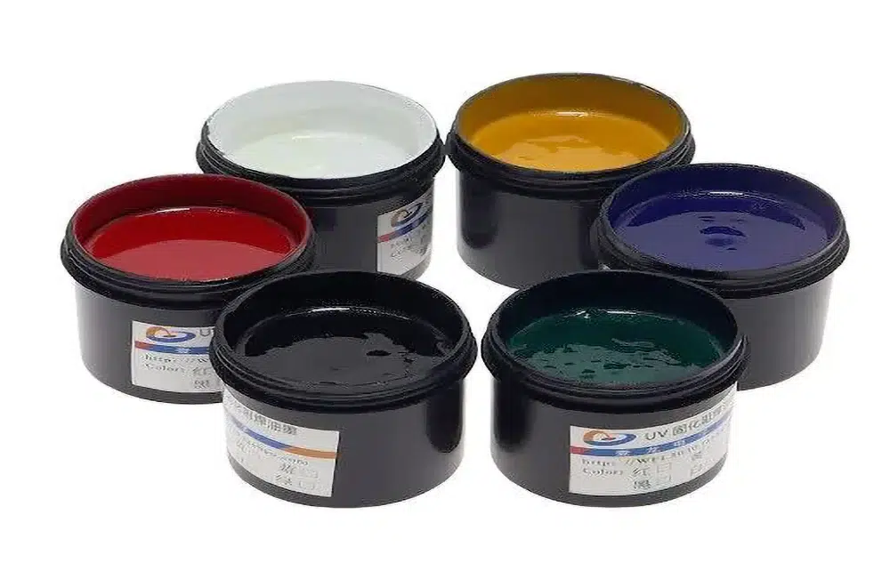
Several solder mask types suit hobbyist workflows, with liquid photoimageable solder mask (LPSM) being the most popular for home use due to its precision and UV curing. LPSM comes as a liquid that you apply, expose to UV light through a photomask, and develop to reveal pads. Dry film solder mask (DFSM) offers another option, involving lamination of a pre-formed film followed by exposure and development, ideal for flat boards. Epoxy-based liquid masks provide a simpler brush-on alternative that air-dries or bakes, though they lack the resolution of photoimageable types. Each type balances ease, cost, and performance, with LPSM favored for fine-pitch traces common in modern electronics.
Hobbyists select based on project complexity; simple single-sided boards work well with epoxy paints, while multi-layer prototypes demand LPSM for accuracy. Thickness typically ranges from 15 to 35 microns in professional specs, a guideline hobbyists can approximate for insulation. Colors like green dominate for visibility, but matte black or blue options reduce glare in optical projects. Availability in small kits makes these accessible via hobby suppliers. Understanding these distinctions ensures the right choice for reliable DIY PCB protection.
Preparing Your PCB for Solder Mask Application
Proper preparation is the foundation of successful DIY solder mask application, starting with a clean, etched PCB free of residues. Degrease the board using isopropyl alcohol or acetone to remove oils, followed by a rinse in distilled water and drying with compressed air. Inspect for undercuts or pits in the etch, as these trap mask material and cause defects. Abrade the copper lightly with fine steel wool if needed to promote adhesion, then clean again. Bake the board at low heat around 100 degrees Celsius for 30 minutes to drive off moisture, preventing bubbles during application. This step aligns with preparation guidelines in standards like IPC-6012 for rigid printed boards.
Mask off fiducials or test points if they require bare copper. Ensure even lighting in your workspace to avoid shadows during inspection. Label the board side to prevent mix-ups in double-sided applications. Patience here pays off by ensuring uniform coverage later. A well-prepared surface mimics factory processes, boosting hobbyist results.
Step-by-Step Guide to Simple DIY Solder Mask Application
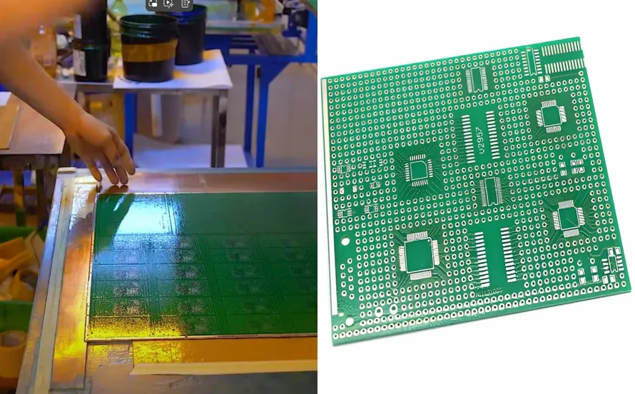
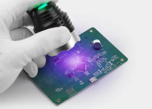
Begin with the liquid photoimageable method, the simplest for precise hobbyist work. Coat the PCB evenly using a foam roller or spin coater improvised from a drill, aiming for uniform thickness. Place a printed transparency film as a photomask over the wet mask, aligning pads perfectly with traces. Expose under a UV lamp for 5 to 10 minutes, depending on mask specs, allowing unexposed areas to remain soluble. Develop in a sodium carbonate solution, agitating gently until pads clear, then rinse thoroughly. Cure fully by baking at 150 degrees Celsius for one hour to harden the mask.
For brush-on epoxy masks, stir well and apply thin layers with a fine brush, avoiding globs on pads. Multiple coats build thickness, with sanding between for smoothness. Air-dry overnight or bake to accelerate. Dry film requires vacuum lamination at 40 to 50 degrees Celsius, followed by exposure and stripping. Test a scrap board first to dial in exposure times. These methods keep DIY accessible without specialized gear.
Post-application, inspect for pinholes or thin spots using a magnifying glass under angled light. Touch up small defects with extra mask material. Solder a test joint to verify insulation. IPC-A-600 provides acceptability criteria for coverage, guiding hobbyists on void limits. Final bake enhances adhesion. Your board now boasts professional protection.
Best Practices and Common Mistakes to Avoid in DIY Solder Mask
Adhere to consistent thickness by measuring with a micrometer on test strips, preventing solder wicking or cracking. Work in a dust-free area, using gloves to avoid fingerprints that compromise adhesion. Overexposure in UV processes hardens the entire mask prematurely, so time exposures precisely with a timer. Underdeveloped boards show residue on pads, leading to soldering woes; extend development if needed. Avoid high humidity, as it causes bubbling in liquid masks.
Common pitfalls include misalignment of photomasks, fixed by using registration holes. Excessive baking warps thin boards, so support them evenly. Poor cleaning leaves residues that peel the mask during flexing. Store unused mask in cool, dark places to maintain potency. Following these elevates hobbyist PCBs to reliable standards.
Troubleshooting Common DIY Solder Mask Issues
Pinholes often stem from dust or air bubbles; filter mask liquid and apply in a vacuum bag if possible. Peeling occurs from weak adhesion, remedied by better surface prep or primer coats. Discolored or hazy masks indicate overexposure; reduce UV time incrementally. Sticky residues post-development mean insufficient curing; extend bake cycles. Bridged pads require careful scraping before reapplication.
For dry film delamination, improve lamination pressure. Yellowing in epoxies signals high bake temps; lower to 120 degrees Celsius. Test compatibility with your etchant residues. Systematic troubleshooting keeps projects on track. Patience refines techniques over multiple boards.
Conclusion
DIY solder mask application empowers electronics hobbyists to create durable, professional PCBs at home using simple tools and materials. From preparation to curing, each step builds reliability against environmental threats and assembly errors. Standards like IPC-SM-840 guide performance expectations, adaptable to hobby workflows. Experiment with LPSM or epoxy for your needs, avoiding common pitfalls through practice. This process transforms basic etches into robust circuits, fostering innovation in personal projects. Embrace solder mask to elevate your electronics endeavors.
FAQs
Q1: What is the simplest DIY solder mask for PCB beginners?
A1: Liquid photoimageable solder mask offers hobbyists an easy entry with UV curing and development. Apply evenly, expose through a transparency mask, and develop to expose pads. It provides good resolution for fine traces without complex equipment. Bake to finalize, ensuring insulation for reliable projects.
Q2: Why apply solder mask on homemade PCBs?
A2: Solder mask protects copper from oxidation and shorts, essential for long-term hobbyist boards. It prevents solder bridges during hand assembly, improving reliability. Clear pad definition aids component placement. Even basic application mimics factory quality and boosts durability in prototypes.
Q3: How to avoid bubbles in DIY solder mask application?
A3: Degrease and dry the PCB thoroughly before coating to minimize trapped air. Warm the board slightly to reduce viscosity during application. Use a roller for an even spread without agitation. Develop slowly to let bubbles escape, keeping the mask smooth for better PCB performance.
Q4: Can hobbyists use dry film for solder mask?
A4: Yes. Dry film solder mask works for DIY with lamination and UV exposure. Laminate at controlled heat, align the film, expose, and strip unexposed areas. It offers uniform thickness ideal for flat boards. Cure fully for adhesion to achieve precise, consistent results.
References
IPC-SM-840E — Qualification and Performance Specification for Permanent Solder Mask. IPC, 2010
IPC-6012E — Qualification and Performance Specification for Rigid Printed Boards. IPC, 2015
IPC-A-600K — Acceptability of Printed Boards. IPC, 2020


