Dimensional expansion and shrinkage in printed circuit boards are inherent outcomes of material thermomechanical behavior compounded by process-induced stresses. The magnitude and direction of change depend on the base materials, copper distribution, and the thermal and mechanical history the panel experiences across fabrication and assembly.
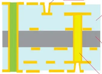
Taking high-density interconnect (HDI) constructions as an example, the laminate stack is broadly composed of roughly 70% prepreg (PP) and 30% copper. Prepreg contracts after exposure to elevated temperatures—noticeably above about 145 °C, but also to a lesser extent around 60–90 °C—while copper can plastically elongate under tensile loading. These distinct responses interact during cutting, imaging, drilling, lamination, laser processing, via plugging, solder mask, plating, and even reflow, yielding the dimensional changes observed in production.
Cause 1: Cutting (Panel Preparation)
Cutting can introduce measurable dimensional change before imaging even begins. Key contributors include:
-
Mechanical stress. Cutting tools impart localized forces that deform copper and the resin/glass substrate. Copper's ductility means tensile loads can cause plastic elongation, locally increasing dimensions.
-
Frictional heating. Tool–panel friction can create localized temperature rise. If temperatures approach the PP's sensitive range (about 60–90 °C) or exceed ~145 °C, the prepreg may contract.
-
Residual stress release. Lamination and cure often leave internal stresses trapped in the panel. Cutting can abruptly relieve these stresses, causing localized dimensional relaxation or distortion.
-
Tool wear and machine accuracy. Worn blades and poor cutting precision produce rough edges and geometric inaccuracy, degrading registration in downstream drilling or imaging and amplifying apparent expansion/shrinkage.
A practical mitigation is to bake panels at 170 °C for 4 hours after cutting and before further processing. This stress-relief bake reduces lot-to-lot variation of the R value (dimensional scale factor) used for compensation. Comparative data versus unbaked controls shows a clear improvement in the R value related to lamination-induced expansion/shrinkage.
Cause 2: Pattern Transfer (Imaging)
Pattern transfer can alter panel dimensions for both material-related and process-related reasons:
Material factors
- Base laminate composition. Epoxy resin and glass fabric expand with temperature and can swell with moisture. Different laminate suppliers and batches can exhibit different residual stress states, leading to inconsistent dimensional change after imaging.
- CTE mismatch between copper and substrate. Copper expands differently than FR-4. Thermal and chemical exposures during imaging can drive nonuniform expansion/shrinkage at the copper–dielectric interface.
Process factors
- Thermal excursions. Exposure, post-exposure bake, development, and etch introduce heat and chemistry. Temperature variations can induce local expansion or contraction. Dry/wet film can also shrink during polymerization after exposure.
- Chemical interaction. Cleaners and etchants can cause micro-etching, swelling, or moisture uptake, altering dimensions.
- Mechanical loading. Lamination of dry film, squeegee pressure, and transport tension can introduce stress, which later relaxes and changes panel size.
Environmental factors
- Ambient temperature and humidity. Fluctuations drive thermal and hygroscopic expansion, especially during storage between imaging steps.
- Storage conditions after cutting. Delays before imaging allow moisture uptake and stress relaxation, shifting the dimensional state.
Residual stress release
- Prehistory of the laminate. Pressing, cutting, and handling can embed internal stresses. Chemical and thermal steps during imaging accelerate stress release and dimension change.
Pre-clean. A single PUMICE scrub has been observed to increase panel size by approximately 2 mil. Representative measurement data is shown below.
Exposure. The actual phototool value used for exposure typically differs from the requested value by up to ±1 mil, within allowed tolerance.
Metrology correlation. Correlation across three in-plant 2D vision measuring systems and a 3D CMM shows the solder mask 2D system aligns closely with the CMM. The phototool-room and pattern-transfer 2D systems differ by about 0.005% (~1 mil) relative to the CMM in this data set.
Cause 3: Lamination
Lamination is one of the most influential stages for dimensional change in multilayer boards.
Thermal stress and post-cure contraction
- Resin cure and cooling. During lamination, resin polymerizes under heat and pressure. Upon cooling, thermal contraction and internal stress development often yield net shrinkage.
- Glass transition temperature (Tg). When lamination temperatures approach or exceed Tg, resin softening and flow increase. After cooling through Tg, greater contraction can occur.
Material mismatch
- CTE differences. Copper's CTE is around 17 ppm/°C; FR-4 is about 12–16 ppm/°C in-plane and 50–70 ppm/°C through thickness. Differential contraction during cool-down can cause warpage and local dimensional change.
- Layer asymmetry. Uneven copper distribution drives unbalanced stress and shape change after pressing.
Press parameters
- Temperature/pressure/time control. Excess heat or uneven pressure increases resin flow and subsequent contraction; insufficient time risks incomplete cure and unstable dimensions.
- Ramp rates. Rapid cool-down traps higher residual stress, increasing edge or local distortion.
Registration and layer shift
- Pre-existing inner-layer change. Any imaging-induced shrink/expansion carries into the stack-up and accumulates.
- Slip during pressing. Resin flow can slightly shift inner copper relative to the dielectric under pressure.
Environment and downstream processes
- Humidity uptake. Moisture-sensitive materials can swell after pressing or shrink upon drying.
- Post-lamination machining. Drilling and routing release stress and may induce secondary distortion.
Process sensitivity example. In one case, version B5 of a motherboard exhibited approximately 0.01% less shrink per press cycle versus version B4, increasing the outer-layer scaling ratio accordingly.
Cause 4: Laser Processing
Laser drilling and structuring can also alter panel dimensions:
-
Thermal stress. Localized laser heating causes momentary expansion; upon cooling, residual stress can leave permanent contraction or distortion. Copper–dielectric CTE mismatch intensifies interlayer stress and positional shift.
-
Material ablation and carbonization. High-energy pulses may ablate resin or glass and form microcracks or carbonized regions. These defects disrupt material uniformity and dimensional stability.
-
Process energy and focus control. Excess energy or poor focus over-heats the stack, increasing shrinkage; inadequate energy requires multiple passes, compounding thermal load.
-
Multilayer interactions. Laser processing may alter adhesion between inner copper and dielectric; subsequent pressing and stress release can change dimensional ratios.
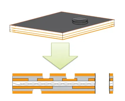
As an example, dimensional ratio change before and after black-oxide treatment was about 0.003% in the data set below.
Cause 5: Via Plugging (Hole Fill)
Via plugging and embedded fill processes can induce both local and global dimensional changes:
-
Cure shrinkage. Resin-based plugging materials contract during polymerization, pulling on the plated hole walls and altering overall dimensional state. Material shrinkage rates differ from the laminate, creating local stress fields.
-
CTE mismatch. Different CTEs between the plug material and substrate generate thermal stresses across thermal cycles.
-
Process uniformity. Underfill or overfill leads to uneven stress; squeeze-out that solidifies against adjacent circuitry can produce local expansion/shrinkage. Unstable cure conditions (time/temperature) increase dimensional variability.
-
Interaction with multilayer pressing. In HDI and multilayer builds, resin flow and cure during subsequent presses can change copper–dielectric adhesion and shift the overall shrink rate.
Observed trends include:
- Post-plug bake. Across different board thicknesses, baking after plugging resulted in net shrinkage: X-axis shrink of approximately 0.003%–0.013% and Y-axis shrink of approximately 0.001%–0.011%.
- Scrubbing. Single versus double mechanical scrub showed small differences, both trending toward expansion: X-axis +0.000%–0.004%, Y-axis +0.001%–0.005%.
- Embedded fill. Through the embedded fill flow, in-process panels expanded: X-axis approximately +0.002%–0.013%, Y-axis approximately +0.009%–0.021%.
Cause 6: Solder Mask
The solder mask process also influences finished dimensions:
-
Ink cure stress. Thermal cure drives polymerization and ink shrinkage, which loads the panel. Nonuniform oven temperature or film thickness can create localized deformation and overall instability.
-
CTE mismatch. Solder mask ink and FR-4 expand and contract differently, producing warpage or dimensional change during heat/cool cycles.
-
Pre-clean impact. Mechanical or chemical pretreatments improve adhesion but excessive scrubbing can micro-damage the surface and shift dimensions; some panels show slight expansion after scrub.
-
Exposure and develop. Chemistry penetration and swelling during develop can cause minor expansion, followed by shrink as the ink cures.
-
Stackup interactions. When combined with via plugging and multilayer lamination, the cumulative stress can amplify expansion/shrinkage.
In measured comparisons before and after solder mask bake, dimensions typically decreased by approximately 0.008%–0.016%.
Relative Contribution Across Processes
From aggregated in-plant data, the most significant contributors to dimensional change tend to be lamination and plating, with the largest net shrink commonly observed in the first and second lamination cycles, plating, and solder mask cure.
Mitigation and Process Control Suggestions
- Bake after cutting to relieve internal stress and stabilize the R value used for dimensional compensation.
- Tightly control imaging parameters (phototool compensation, exposure energy, PUMICE scrub) and correlate metrology systems to minimize measurement-induced variability.
- Balance inner-layer copper and follow controlled lamination temperature, pressure, time, and ramp rates. Avoid asymmetric stackups when possible.
- Optimize laser parameters (energy, focus, pulse frequency, scan speed) to limit thermal damage and cumulative heat exposure.
- Standardize via plug materials and cure profiles; monitor fill uniformity and manage post-plug bake to reduce stress.
- Control solder mask thickness, bake uniformity, and pre-clean to minimize ink-induced shrinkage.
- During SMT reflow, panels tend to shrink, and larger panels shrink more. This can degrade second-side placement accuracy. For products at second order and above, it is advisable to keep the SET size no greater than 7 inches.
Summary
- Dimensional expansion and shrinkage are multi-factor outcomes; stabilizing the finished size requires coordinated control across the entire process flow.
- Laminate compensation (R value) is established for a normal, controlled process. Each station should strictly follow standard work practices and verify the first article to reduce rework and variability.
- Pattern transfer and drilling are the key control points for adjusting abnormal scaling ratios and directly determine finished dimensions. These stations require special focus.