










PCB Vias Plugging: Manufacturing Process, Failure Modes, and Reliability Impact
What This Video Covers
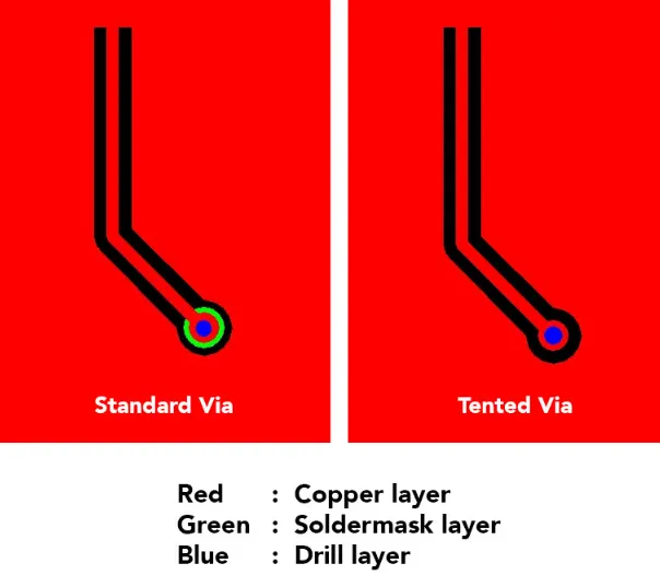
This video explains the critical role of via plugging in modern PCB fabrication and SMT assembly. After drilling and copper plating, vias are filled with solder mask ink or epoxy to improve surface planarity, prevent solder wicking during assembly, and enhance overall board reliability.
Key manufacturing steps include pressing plugging material into plated vias followed by partial curing. While effective for solder control and cleanliness, incomplete plugging can trap air, leading to voids, outgassing, or cracking during thermal cycling — common failure modes in high-reliability applications.
The video provides practical design considerations: selecting appropriate via sizes within manufacturer capabilities, inspecting for sink marks or incomplete fill, and choosing advanced options like via-in-pad with epoxy filling plus copper capping for high-density designs.
These techniques are especially important for HDI PCB, Rigid-Flex PCB, and multilayer boards used in automotive electronics, medical devices, and industrial control systems where thermal management and long-term reliability are non-negotiable.
For your next project requiring precise via handling and reliable assembly, request an instant PCB quote or explore professional turnkey PCB assembly services.
Key Highlights
- Via plugging with solder mask or epoxy prevents solder intrusion, improves planarity, and reduces assembly defects in plated through holes.
- Poor plugging risks air entrapment and cracking during thermal cycling, making via size and process control essential design considerations.
- For high-density boards, via-in-pad with epoxy fill and copper capping offers superior performance over standard solder mask plugging.
Critical Role of Via Plugging After Drilling and Plating
After the via is drilled and electroless or electrolytic copper plating forms the conductive barrel, the open hole presents multiple process risks. During subsequent solder-mask application or SMT reflow, liquid solder can be drawn into the via by capillary action, depleting the pad surface and creating insufficient joint volume. Residual flux or cleaning solvents can also become trapped, leading to ionic contamination and electrochemical migration over time.
Plugging seals the barrel, restores a flat topography for fine-pitch components, and blocks these pathways. In production, the plugging material is forced into the via under controlled pressure and then partially cured so that excess material can be planarized. Full curing follows later process steps. Proper execution maintains electrical continuity while eliminating the open volume that would otherwise collect contaminants or expand under thermal stress.
In multilayer and HDI constructions the number of vias multiplies, making consistent plugging essential for both yield and long-term field reliability. Boards destined for automotive or medical use routinely specify plugging because thermal-cycling profiles and vibration loads quickly expose any unfilled or partially filled vias as crack-initiation sites.
Solder Mask Versus Epoxy Filling: Process Differences and Production Trade-offs
Two primary materials are used for PCB vias plugging. Liquid photoimageable solder mask is the lower-cost option. It is applied by screen printing or spraying and then vacuum-assisted or mechanically pressed into the vias. Because solder-mask viscosity is relatively low, complete fill of high-aspect-ratio holes is difficult; residual air pockets are common. After curing, the surface may show sink marks or dimples that affect solder-paste printing.
Epoxy plugging compounds are higher-viscosity, non-conductive resins formulated for vacuum or pressure filling. They achieve near-100 % fill even in smaller-diameter vias, cure to a hard, thermally stable plug, and can be planarized and copper-capped. The process requires dedicated plugging equipment, longer cycle times, and tighter process control, increasing cost relative to solder-mask plugging.
Selection depends on via diameter, board thickness, and end-use requirements. Solder-mask plugging is adequate for moderate-density boards where only solder-wicking prevention is needed. Epoxy filling is specified when planarity under BGA or QFN packages, thermal conductivity, or absolute void-free performance is required.
| Parameter | Solder-Mask Plugging | Epoxy Filling + Copper Cap |
|---|---|---|
| Typical via diameter range | ≥ 0.3 mm | 0.1–0.5 mm |
| Fill completeness | 70–90 %, possible voids | >95 %, near void-free |
| Surface planarity | Moderate; sink marks common | Excellent after planarization |
| Thermal/electrical impact | Minimal | Improved heat path when capped |
| Cost impact | Low | Moderate to high |
| Preferred applications | Standard multilayer, cost-sensitive | HDI, via-in-pad, automotive, medical |
Common Manufacturing Defects from Incomplete Via Plugging
Incomplete fill is the most frequent defect observed in production. Air trapped during plugging expands during reflow or subsequent thermal cycling, forming voids that act as stress concentrators. These voids can propagate into cracks that sever the copper barrel or delaminate the pad, causing open circuits or intermittent failures.
Sink marks appear when the plugging material shrinks during cure and leaves a depression on the surface. On fine-pitch pads the depression creates uneven solder-paste volume, increasing the risk of tombstoning or insufficient wetting. Outgassing from residual solvents or incompletely cured resin can also contaminate nearby solder joints, producing voids inside the intermetallic layer.
In high-reliability screening, cross-sectioning and microvia X-ray inspection routinely reveal these defects. Boards that pass electrical test at room temperature may still fail after 500–1000 thermal cycles between –40 °C and 125 °C if plugging quality is marginal. Process controls that monitor vacuum level, material viscosity, and cure profile are therefore mandatory for any design that specifies via plugging.
Design Rules and Via Size Limits for Reliable Plugging
Manufacturer capabilities define the practical window for successful plugging. Most fabricators require a minimum finished via diameter of 0.2–0.3 mm for reliable solder-mask plugging and can handle down to 0.1 mm with epoxy systems when aspect ratios stay below 8:1 to 10:1. Larger vias (>0.5 mm) are more difficult to fill completely without voids and may need multiple plugging passes.
Designers must also account for the annular ring and copper plating thickness; excessive plating reduces the effective hole diameter and can leave an unfilled cusp at the barrel wall. Stack-up symmetry is important: unbalanced copper distribution increases warpage during the thermal cure of the plugging material, further aggravating incomplete fill.
Clear documentation of plugging requirements—whether solder mask only, epoxy fill, or epoxy fill plus copper cap—must appear in the fabrication notes. Omitting this information forces the manufacturer to apply default processes that may not meet the reliability targets of the end application.
Via-in-Pad with Epoxy Fill and Copper Capping for High-Density Boards
When vias are placed directly under BGA or QFN pads, standard solder-mask plugging is rarely sufficient. Residual dimples or incomplete seals allow solder to wick into the via during reflow, starving the joint and creating open or high-resistance connections. The preferred solution is non-conductive epoxy fill followed by planarization and electrolytic copper capping.
The capped surface presents a flat, solderable pad identical to a solid copper land. This approach eliminates solder wicking, improves thermal dissipation from the component, and supports the finer via pitches required by HDI and microvia constructions. The process adds cost and requires tighter registration tolerances, yet the improvement in first-pass assembly yield and long-term reliability usually justifies the investment for automotive, medical, and industrial control boards.
Designers should confirm that the chosen fabricator can perform both the plugging and the subsequent copper capping in a single controlled sequence; separating these steps increases the risk of contamination or misalignment.
FAQ
Q1: When should via plugging be specified in PCB designs?
A1: Use via plugging whenever solder control, surface planarity, or via protection is required — especially under BGA packages, in high-density HDI layouts, or for boards facing thermal cycling in automotive and industrial applications.
Q2: What are the limitations of standard solder mask via plugging?
A2: It can trap air causing voids or sink marks, may not fully seal larger vias, and offers limited thermal/electrical performance compared to epoxy-filled and capped vias in demanding multilayer designs.
Q3: How does via plugging affect SMT assembly reliability?
A3: Proper plugging prevents solder wicking into vias, reduces tombstoning risk, and ensures cleaner pads, significantly improving first-pass yield and long-term joint reliability in high-volume production.
Q4: What via aspect ratio is typically required for reliable epoxy plugging?
A4: Most production processes achieve consistent, void-free epoxy fill when the aspect ratio (board thickness divided by finished hole diameter) remains at or below 10:1. Higher ratios increase the probability of trapped air and incomplete fill, requiring specialized vacuum-assist equipment or multiple filling passes that raise cost and cycle time.
Q5: Can plugged vias still be used for thermal management?
A5: Non-conductive epoxy or solder-mask plugs provide only modest thermal improvement because the fill material has significantly lower thermal conductivity than copper. Heat transfer through a plugged via therefore remains limited compared with an open or copper-filled barrel.
Ever wondered why tiny holes on a PCB sometimes cause soldering failures?
That's where via plugging comes in.
After drilling and copper plating, solder mask ink is pressed into the via and partially cured.
Via plugging helps improve assembly reliability and keeps the via better protected.
But plugging is not perfect.
Poor filling can trap air, causing voids or cracking during thermal cycling.
So here's the key:
Use via plugging when solder control, cleanliness, or surface planarity matters.
Keep via sizes within your manufacturer's supported plugging range.
And check for voids, sink marks, or incomplete filling before assembly.
For high-density boards, consider via-in-pad with epoxy filling and copper capping instead of simple solder mask plugging.





