Introduction
Solder mask plays a critical role in protecting printed circuit boards from environmental factors and preventing solder bridges during assembly. In through-hole assembly processes, where components are inserted into plated through-holes and soldered via wave or selective methods, solder mask application presents distinct hurdles. Larger hole diameters and the dynamics of molten solder flow amplify risks like wicking and flux entrapment. Engineers often encounter issues with solder mask through hole interactions that can compromise joint integrity and board reliability. This article delves into these challenges, focusing on solder mask tenting through hole and solder mask plugging through hole techniques, and offers practical solutions grounded in industry practices. Understanding these elements ensures smoother through hole assembly and higher yield rates.
Understanding Solder Mask in Through-Hole Assembly
Solder mask is a thin polymer layer applied to the PCB surface, typically after copper etching and plating, to insulate traces and define solderable areas. In through-hole assembly, it must precisely expose component pads and holes while covering surrounding copper to avoid shorts. The mask bridges over non-component vias to seal them, but plated through-holes for leads remain fully open. This selective coverage demands high precision, as misalignment can lead to mask encroachment on pad lands, reducing solder fillet formation. Liquid photoimageable (LPI) solder mask dominates due to its resolution for fine features, though dry film alternatives suit thicker applications.
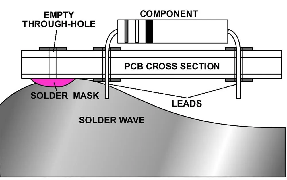
The relevance stems from wave soldering's aggressive thermal and fluid dynamics, where unprotected vias draw solder upward, depleting joint volume. Flux residues trapped in open holes accelerate corrosion over time. Proper solder mask through hole management enhances mechanical strength, thermal performance, and longevity in demanding electric applications. Without it, boards risk failures during insertion or reflow preheat stages common in mixed assemblies.
Key Challenges in Solder Mask Application for Through-Hole Boards
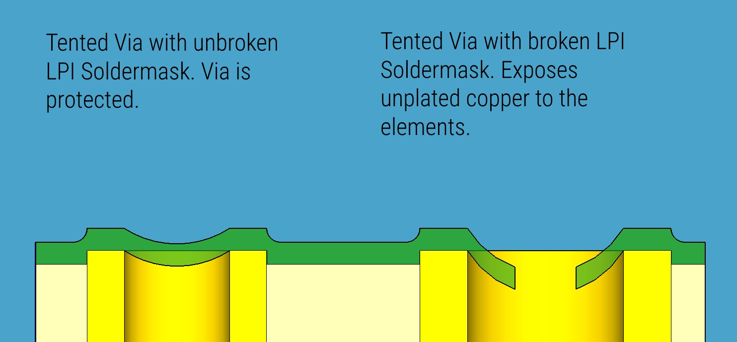
One primary challenge involves solder mask tenting through hole, where the mask stretches thinly over via openings without apertures in the artwork. For vias under 0.35 mm finished diameter, tenting holds reliably, but larger holes in through-hole designs risk rupture during curing or thermal cycling. This exposes the barrel to flux, causing ionic contamination and electromigration. In wave soldering, broken tents allow solder wicking, which starves adjacent component joints of material and creates voids.
Solder mask plugging through hole addresses sealing but introduces voids from air entrapment during ink fill. Incomplete plugs pop during reflow, ejecting material onto components and causing shorts. Plugged vias also face outgassing if moisture penetrates before capping. Mask adhesion fails on contaminated surfaces, leading to peeling that exposes traces to handling damage.
Component lead insertion compounds issues, as raised mask lips around holes snag pins, misaligning parts. Excessive mask thickness exacerbates warpage over multi-layer boards, stressing tents. These factors demand troubleshooting focused on process controls and design tweaks.
Mechanisms Behind Solder Mask Issues in Through-Hole Assembly
Tenting relies on mask viscosity and exposure to form a membrane spanning the annular ring. LPI flows into small features but thins over holes, with UV crosslinking locking the shape. Thermal expansion mismatch between mask, copper, and laminate induces stress cracks, per IPC-6012 performance specs for rigid boards. Wave soldering's preheat expands trapped air under tents, ballooning or bursting them if not vented properly.
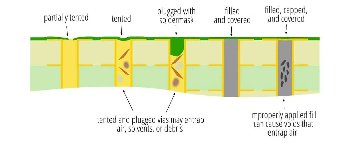
Plugging involves screen-printing conductive or non-conductive ink into holes, followed by tenting and curing. Shrinkage during polymerization creates voids, especially in deeper barrels typical of through-hole vias. IPC-4761 outlines via protection types, noting Type IV (plugged and capped) suits high-reliability needs but requires vacuum assist for uniform fill. Flux activation in assembly hydrolyzes residues in imperfect plugs, generating gases that delaminate the mask.
Mask encroachment occurs from overexposure or poor registration, shrinking openings below lead-to-hole ratios. This demands precise panelization and fiducials for alignment.
Practical Solutions and Best Practices
Start with design rules: Maintain 0.1 mm minimum solder mask clearance from pad edges to ensure full exposure. For vias needing tenting, limit finished hole size to 0.3 mm maximum for single-side tenting, tenting both sides where possible to balance stress. Specify non-tented component holes explicitly in fabrication notes to avoid accidental coverage.
Opt for LPI solder mask for superior tent resolution over epoxy screens in high-volume through hole assembly. Implement double-sided tenting for signal vias to block flux from both wave and component sides. For critical plugs, use conductive epoxy followed by plated caps, reducing thermal mass.
Process controls include plasma cleaning pre-mask application to boost adhesion. Cure profiles with gradual ramps minimize tent stress. IPC-A-600 acceptability criteria guide inspection, rejecting pinholes over 0.13 mm or lifts exceeding 25% coverage.
In assembly, preheat boards slowly to outgas plugs before wave immersion. Selective soldering for dense areas preserves tent integrity.
Troubleshooting Common Through-Hole Solder Mask Defects
Engineers troubleshooting tent failures inspect for thin spots via cross-sectioning or dye penetrant tests. Ruptures often trace to oversized vias; resize or plug instead. Wicking shows as icicles in joints; counter with full tenting or filled vias.
Plug voids appear as dimples post-cure; vacuum printing resolves this. Insertion snags from mask lips require thinner applications or post-etch profiling. Adhesion loss signals surface prep issues; etch back copper lightly.
Mixed SMT/THT boards benefit from plugged vias under BGAs to prevent reflow flux bleed into through-hole zones. Monitor via protection per IPC-4761 Type VI for filled and covered structures in high-density designs.
Conclusion
Navigating solder mask through hole challenges in through hole assembly requires balancing protection with accessibility. Tenting and plugging offer tailored defenses against wicking, entrapment, and reliability killers. Adhering to proven design rules, process tweaks, and standards like IPC-4761 yields robust boards. Engineers gain confidence by specifying protections upfront, minimizing rework and boosting assembly yields. Prioritizing these practices elevates PCB performance in electric engineering applications.
FAQs
Q1: What is solder mask tenting through hole, and when should it be used in through hole assembly?
A1: Solder mask tenting through hole covers via openings with a thin mask layer without apertures, sealing against flux and solder. Use it for signal vias under 0.35 mm diameter to prevent wicking during wave soldering. It suits most through hole assembly boards but avoid on component holes. Specify both sides for balanced protection, ensuring annular rings exceed 0.15 mm for integrity.
Q2: How does solder mask plugging through hole improve through hole assembly reliability?
A2: Solder mask plugging through hole fills vias with ink before capping, blocking moisture and flux completely. It prevents outgassing and voids common in tenting alone, ideal for mixed assemblies. Vacuum-assisted filling ensures uniformity, per via protection guidelines. This enhances joint strength by maintaining solder volume on pads. Inspect for dimples post-cure to confirm quality.
Q3: What are common solder mask through hole clearance issues in through hole assembly?
A3: Insufficient clearance causes mask overlap on pads, hindering lead insertion and solder wetting. Aim for 0.1 mm minimum expansion around holes. Misregistration from artwork errors worsens this; use fiducials for alignment. Troubleshoot by measuring openings post-mask. Proper rules prevent snags and ensure fillet formation.
Q4: Can solder mask tenting through hole fail during wave soldering, and how to mitigate?
A4: Yes, tents rupture from thermal expansion or thin spots, allowing wicking. Mitigate with smaller vias, LPI mask, and both-side tenting. Preheat controls reduce stress. Per acceptability standards, reject pinholes. Plug critical vias for redundancy in high-reliability through hole assembly.
References
IPC-4761 — Design Guide for Protection of Printed Board Via Structures. IPC
IPC-6012E — Qualification and Performance Specification for Rigid Printed Boards. IPC, 2017
IPC-A-600K — Acceptability of Printed Boards. IPC, 2020


