 00:51
00:51
Solder Mask Plugging
Solder mask plugging is a critical technique in printed circuit board (PCB) design and manufacturing that involves filling vias or through-holes with solder mask material to prevent solder flow, contamination, or electrical issues during assembly. This process enhances the reliability and performance of PCBs by creating a smooth, protected surface that minimizes defects such as bridging or short circuits. For engineers, designers, and hobbyists searching for information on solder mask plugging, this tag serves as a comprehensive resource, covering everything from basic principles to advanced implementation strategies. Understanding solder mask plugging starts with its role in via protection. In high-density PCBs, vias can inadvertently allow solder to wick through, leading to assembly failures or reduced signal integrity. By plugging these vias with non-conductive solder mask, manufacturers achieve better insulation and a more uniform board topography, which is essential for applications like BGA (ball grid array) components or multi-layer boards. Practical benefits include improved thermal management, reduced risk of corrosion, and compliance with industry standards such as IPC-4761, which outlines via protection types like tenting, filling, or plugging. For those implementing this in their projects, best practices involve selecting the appropriate plugging method based on board complexity and environmental demands. Epoxy-filled plugging offers superior durability for harsh conditions, while simpler mask plugging suits cost-sensitive designs. Engineers should consider factors like via size, aspect ratio, and curing processes to ensure optimal results. Testing for voids or incomplete fills through cross-section analysis can prevent long-term failures. This tag aggregates articles that delve into these topics, providing step-by-step guides, case studies, and troubleshooting tips. Whether you are optimizing a prototype or scaling production, the insights here can help refine your PCB fabrication approach for greater efficiency and reliability.
Video Guide
-
00:51
Technical Articles
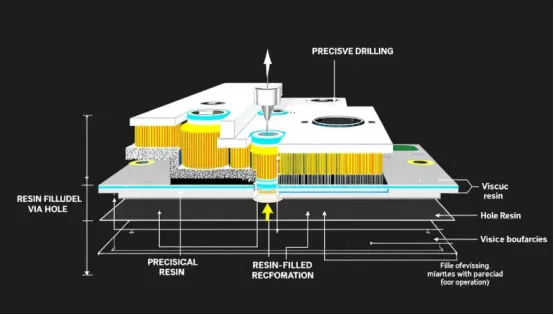
Which Vias Need Resin Plugging? Real Engineer Questions from Production
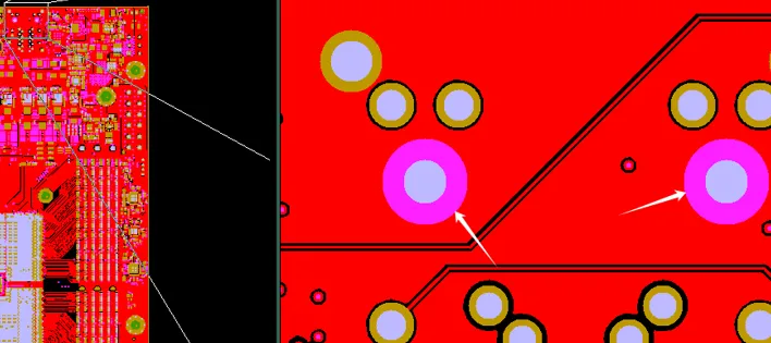
14 Layer TG170 PCB Manufacturing Review for Impedance and Resin Plugging
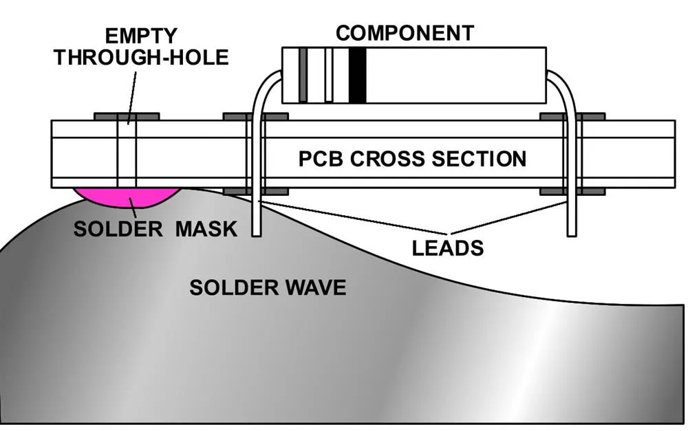
Solder Mask for Through Hole Assembly: Unique Challenges and Solutions

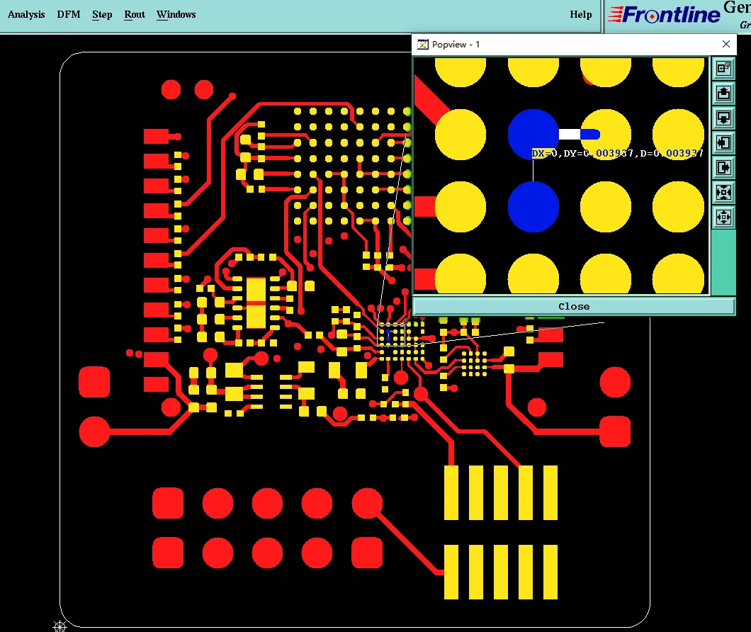
Resin Filled Via & Blind Via Issues in 6-Layer 2nd Order HDI PCB CAM Review
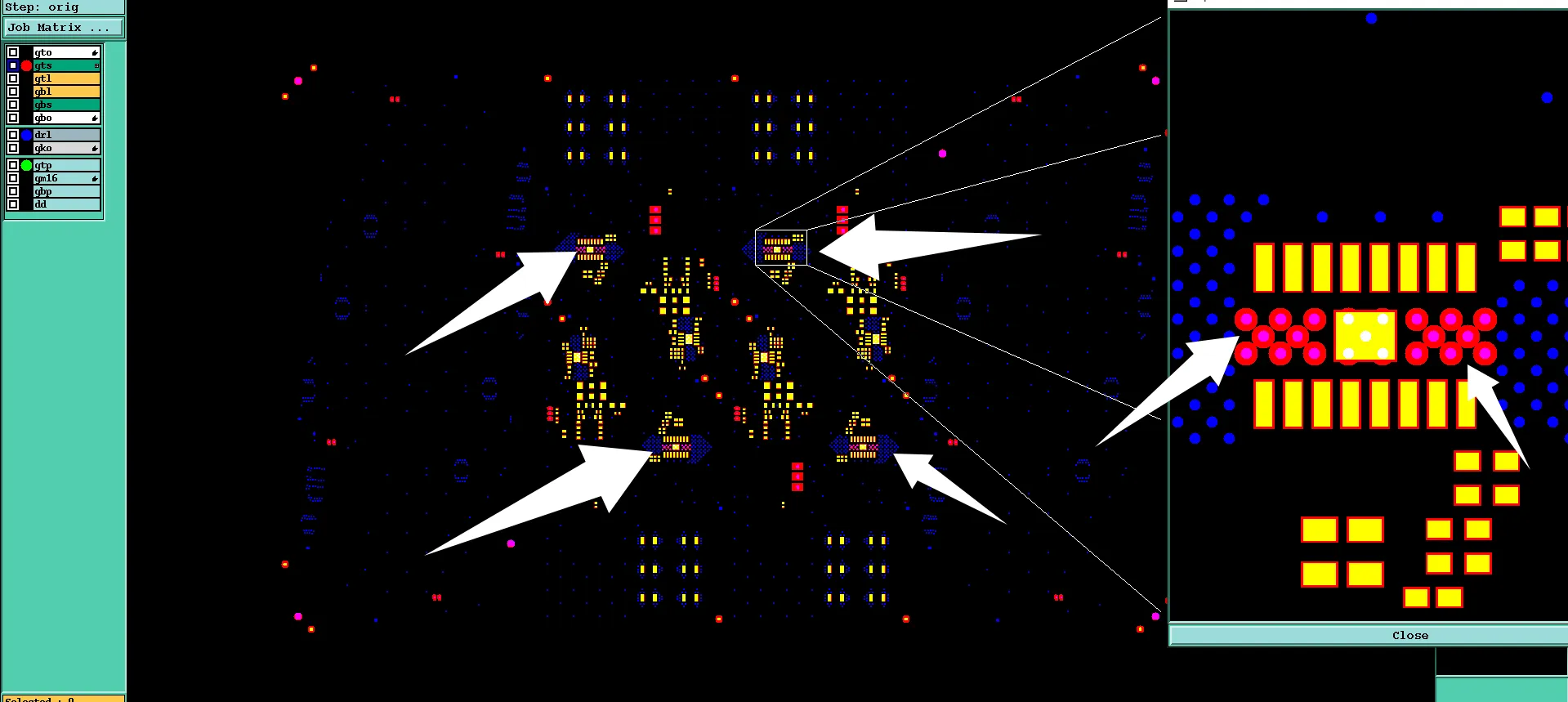
Resolving Tented Via vs Open Via Mismatches in PCB Manufacturing
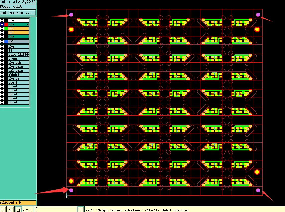
Tented Via vs Open Via Conflict Resolved in 2-Layer FR4 PCB
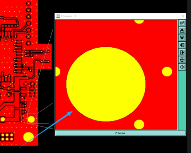
Preventing Exposed Copper and Via Plugging Risks in a Compact 4-Layer FR4 PCB